SOM-4418
From FriendlyELEC WiKi
Revision as of 07:30, 11 August 2020 by Yonganch (Talk | contribs) (→Diagram, Layout and Dimension)
Contents
1 Introduction
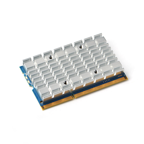
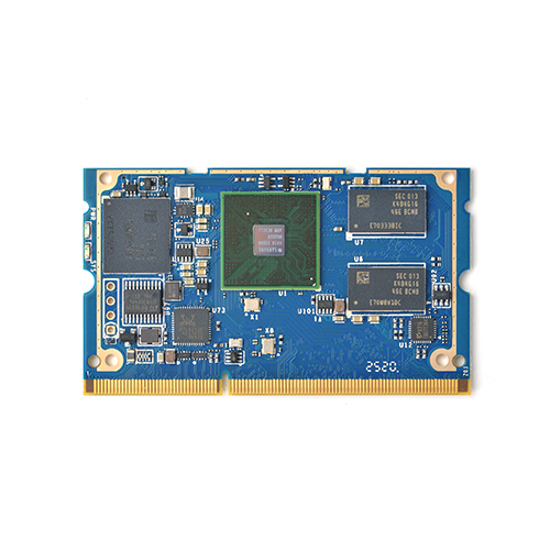
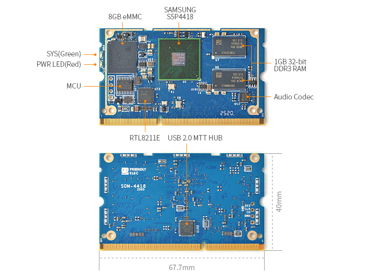
- The SOM-4418 quad core Cortex A9 core board is designed and developed by FriendlyELEC for professional and enterprise users. It uses the Samsung Quad Core Cortex-A9 S5P4418 SoC with dynamic frequency scaling up to 1.4GHz. SOM-4418 has 8G eMMC, 1GB 32bit-DDR3, GigE, and audio codec. To avoid overheat issues the SOM-4418 has a heat sink with mounting posts.
- The SOM-4418 has LVDS and RGB-LCD interface, support resistive touch and capacitive touch.
- The SOM-4418 also has USB HOST, UARTs, I2Cs, SPI, PWM, GPIOs etc.
2 Hardware Spec
- SoC:Samsung S5P4418 Quad Core Cortex-A9 with dynamic frequency scaling up to 1.4G Hz
- PMU Power Management: Implemented by an MCU, support solftware power-off, and RTC alarm power-on functions
- System Memory:1GB 32bit DDR3 RAM
- eMMC:8GB
- Ethernet:Gbps Ethernet Port (RTL8211E) with unique MAC, support WOL(Wake On Lan)
- Video Input: MIPI-CSI
- Video Output: HDMI / LVDS / LCD
- Audio: Build in Codec, 2-Chanel headphone output, one Microphone input
- USB: 4 x USB 2.0 Host(Via USB Hub), 1 x USB 2.0 OTG
- GPIO: 13 x GPIOs, 3 x I2Cs, 1 x SPI, 5 x UARTs, 3 x PWMs, 2 x SDIOs
- LED: 1 x power LED , 1 x SYS LED
- Other Resource: 1 x onboard thermistor
- Power: DC 5V/1A
- Heat Sink: Aluminum heat sink
- PCB: Six Layer, ENIG
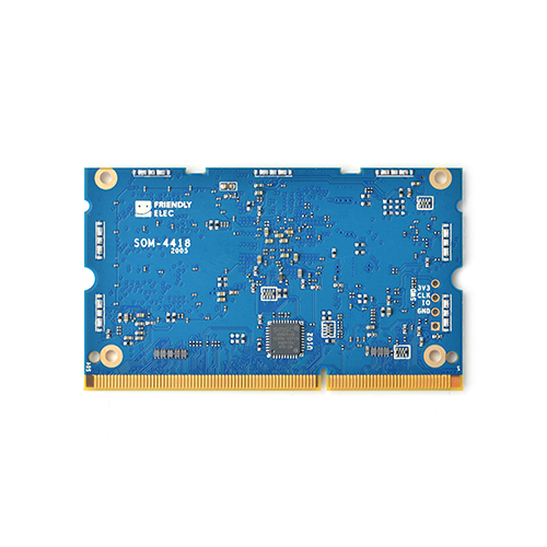
- PCB Dimension: 67.7 mm x 40 mm
- Working Temperature: -40℃ to 70℃
3 Software Features
4 Diagram, Layout and Dimension
4.1 Layout
- 204 Pin Spec
- Socket Type:0.6mm Pitch 204-Pin Standard Type DDR3 SODIMM Socket
Pin# Name Description Pin# Name Description 1 VDD_5V 4.7~5.5V Power Suply input 2 VDD_5V 4.7~5.5V Power Suply input 3 VDD_5V 4 VDD_5V 5 VDD_5V 6 VDD_5V 7 GND 8 GND 9 GND 10 VRTC_IN RTC backup battery(3V)input,backup current is 3.5uA 11 VCC_WIFI_IO(3.3V) MMC1 IO reference power,connect to wifi module IO power input 12 VCC_IO(3.3V) 3.3V out for IO reference 13 MMC1_D0 SDIO1/MMC1, connect to wifi module 14 BOOT_CS Pull low this pin to boot from SD CARD on MMC0 15 MMC1_D1 16 PWRKEY Power key 17 MMC1_D2 18 NRESETIN Hard reset input 19 MMC1_D3 20 AliveGPIO3 GPIO, reserved for RecoveryKey 21 MMC1_CMD 22 EXT_PWR_CTRL Used this pin to control power on/off of the carrier 23 GND 24 MMC0_D0 SDIO0/MMC0, for SD Card 25 MMC1_CLK SDIO1 Clock Out 26 MMC0_D1 27 WL_REG_ON(GPIOB24) GPIOB24, Used as wifi power on control signal 28 MMC0_D2 29 WL_HOST_WAKE(GPIOC17) GPIOC17, Used as wifi wake-up signal 30 MMC0_D3 31 UART1_TX UART1, connect to bluetooth module 32 MMC0_CMD 33 UART1_RX 34 MMC0_CD 35 UART1_nCTS 36 MMC0_CLK 37 UART1_nRTS 38 GND 39 BT_RST_N(GPIOB8) GPIOB8, Used as bluetooth reset 40 MIPI_CSI0_CLKN MIPI CSI Clock 41 BT_WAKE bluetooth wake-up signal 42 MIPI_CSI0_CLKP 43 BT_HOST_WAKE(/NC) Reserved for BT_HOST_WAKE 44 GND 45 LPO_32Khz 32.768kHz output for wifi/bt module 46 MIPI_CSI0_D0N MIPI CSI data0 47 GND 48 MIPI_CSI0_D0P 49 MDI0_P GbE MDI signals 50 GND 51 MDI0_N 52 MIPI_CSI0_D1N MIPI CSI data1 53 MDI1_P 54 MIPI_CSI0_D1P 55 MDI1_N 56 GND 57 GND 58 /NC 59 MDI2_P GbE MDI signals 60 /NC 61 MDI2_N 62 GND 63 MDI3_P 64 /NC 65 MDI3_N 66 /NC 67 GND 68 GND 69 SPEED_LED GbE SPEED LED signal output 70 /NC 71 LINK_LED GbE LINK LED signal output 72 /NC Connector Key 73 GND 74 TP_INT(GPIOC16) I2C signal, connect to touch controller 75 USB_DM4 USB 2.0 host data signal 76 TP_SDA(I2C2_SDA) 77 USB_DP4 78 TP_SCL(I2C2_SCL) 79 GND 80 OneWire(GPIOC15) GPIOC15, used as FriendlyElec LCD OneWire signal 81 USB_DM3 USB 2.0 host data signal 82 GND 83 USB_DP3 84 LCD_CLK RGB LCD Clock signal 85 GND 86 GND 87 USB_DM2 USB 2.0 host data signal 88 LCD_HSYNC RGB LCD horizontal synchronization 89 USB_DP2 90 LCD_VSYNC RGB LCD vertical synchronization 91 GND 92 LCD_DE signal the external LCD that data is valid on the data bus 93 /NC 94 GND 95 /NC 96 LCD_R0 RGB LCD Red data signals 97 GND 98 LCD_R1 99 USB_OTG_D- USB 2.0 OTG data signal 100 LCD_R2 101 USB_OTG_D+ 102 LCD_R3 103 USB_OTG_ID USB 2.0 OTG ID signal 104 LCD_R4 105 VBUS USB 2.0 OTG VBUS 106 LCD_R5 107 VBUS_DRIVE(/NC) Reserved for USB 2.0 OTG VBUS Power Drive Signal 108 LCD_R6 109 HDMI_HPD HDMI Hot plug detect 110 LCD_R7 111 I2C1_SDA I2C1, used as HDMI DDC signal 112 GND 113 I2C1_SCL 114 LCD_G0 RGB LCD Green data signals 115 HDMI_CEC HDMI CEC Signal 116 LCD_G1 117 GND 118 LCD_G2 119 HDMI_TXCN HDMI Clock and data signals 120 LCD_G3 121 HDMI_TXCP 122 LCD_G4 123 GND 124 LCD_G5 125 HDMI_TX0N 126 LCD_G6 127 HDMI_TX0P 128 LCD_G7 129 GND 130 GND 131 HDMI_TX1N 132 LCD_B0 RGB LCD Blue data signals 133 HDMI_TX1P 134 LCD_B1 135 GND 136 LCD_B2 137 HDMI_TX2N 138 LCD_B3 139 HDMI_TX2P 140 LCD_B4 141 GND 142 LCD_B5 143 USB_DM1 USB 2.0 data signal 144 LCD_B6 145 USB_DP1 146 LCD_B7 147 GND 148 GND 149 /NC 150 LVDS_Y3M LVDS signals 151 /NC 152 LVDS_Y3P 153 GND 154 GND 155 /NC 156 LVDS_CLKM 157 /NC 158 LVDS_CLKP 159 GND 160 GND 161 GPIOB31 GPIOs 162 LVDS_Y2M 163 GPIOB30 164 LVDS_Y2P 165 GPIOC7 166 GND 167 GPIOC8 168 LVDS_Y1M 169 GPIOB23 170 LVDS_Y1P 171 GPIOC2 172 GND 173 GPIOC13/PWM1 PWMs 174 LVDS_Y0M 175 GND 176 LVDS_Y0P 177 GPIOC14/PWM2 178 GND 179 GPIOD1/PWM0 180 SPI0_CLK/GPIOC29 SPI 181 I2C2_SDA I2Cs 182 SPI0_MOSI/GPIOC31 183 I2C2_SCL 184 SPI0_MISO/GPIOD0 185 I2C0_SDA 186 SPI0_CS/GPIOC30 187 I2C0_SCL 188 GPIOD8/PPM 189 GPIOB27/HP_DETECT GPIOB27, used as Headphone insert detect 190 UART4_TX/GPIOB29 UARTs 191 AUDIO_GND Headphone output return path 192 UART4_RX/GPIOB28 193 HP_R Headphone output R 194 UART3_RX/GPIOD17 195 HP_L Headphone output L 196 UART3_TX/GPIOD21 197 LINEOUT_R(HP_R) Internal connect to HP_R, reserved for line out R in the future 198 UART2_RX 199 LINEOUT_L(HP_L) Internal connect to HP_L, reserver for line out L in the future 200 UART2_TX 201 MICIN_N Microphone input N 202 UART0_RX Used as Debug console 203 MICIN_P Microphone input P 204 UART0_TX
- Note:
- All VDD_5V Must be connected to get the lowest connection resistance.
- All GND Must be connected for good EMC performance and system stability.
- A 4-layer PCB carrier board is highly recommended.
- For more details refer to the document: SOM-4418-2005-Schematic.pdf
4.2 Board Dimension
- For more details refer to the document: SOM-4418_2005_dxf.zip
5 Notes in Hardware Design
5.1 EEPROM
- The board has an EEPROM(model: 24AA025E48T-I/OT) with a unique MAC. This EEPROM is connected to I2C0 and its address is 0x51 therefore some EEPROM chips cannot be connected to I2C0 which will cause conflicts of addresses.
- In our tests these EEPROM chips cannot be connected to I2C0: 24C04, 24C08 and 24C16. There chips which we tested can be connected to I2C0: 24C01, 24C02 and 24C256
- For more details about EEPROM address issues refer to http://www.onsemi.com/pub_link/Collateral/CAT24C01-D.PDF
6 Schematics & Mechanical drawing
- PCB Dimension(SOM-4418_2005_dxf.zip)
- Schematic(SOM-4418-2005-Schematic.pdf)
- S5P4418 Datasheet (S5P4418_Datasheet_0.1.pdf)


