Smart4418SDK 1305
From FriendlyELEC WiKi
Contents
[hide]1 Introduction


The Smart210/4418 SDK carrier board has rich interfaces and ports. Besides the popular HDMI, USB host, SD card slot, DB9 port, RJ-45 Ethernet port, audio input and output it has onboard EEPROM, buzzer, user keys, GPIO, SDIO which allow users able to fully assess a CPU board. In order for users to conveniently carry it and work with and mount different LCDs we carefully designed the board's layout such that it can work with FriendlyARM's 3.5"LCD, 4.3"LCD, 5"LCD, 7"LCD and 10.1"LCD.
2 Features
Carrier Board Smart210/4418 SDK Standard Version Name Smart210SDK 1305 Dimension 180 x 130(mm) CPU Boards It Works With Smart4418 or Smart210 CPU board Antenna Yes(beside miniUSB) CMOS Camera Interface 20pin 2.0mm pitch double row
DVP Camera interface, ITU-R BT 601/656 8-bitHDMI Output 1 x HDMI A Type, Support HDMI 1.3(Smart210), 1.4a(Smart4418)
Support 1080P30 outputRS232 Serial Port 2 x 3 wire Serial Port(UART0,3), DB9 male connector TTL serial 4 x Serial(UART0,1,2,3), 4pin 2.0mm pitch pin header USB Host 4 x USB type A
brought out via USB 2.0 hub (USB 1.1 compatible)USB Device USB 2.0 1 x MiniUSB Audio Input & Output Support audio recording and play
3.5mm audio jack and MIC pins
onboard MicrophoneEthernet 10/100M Adaptive Ethernet User Key 8 x Key LED 1 x power LED, 2 x GPIO LED for Smart4418 or 4 x GPIO LED for Smart210 RTC Onboard RTC battery(CR1220) Buzzer 1 x PWM buzzer SD Card Slot Pop-up SD card slot LCD Interface 3 x LCD Interface(for different LCD models)
Support FriendlyARM's one-wire touch
Support backlight control
Support capacitive touch
Support RGB888 LCDLCD Mounting Hole for FriendlyARM's 3.5", 4.3", 5", 7", 10.1" LCDs MIPI-DSI/LVDS 30pin, 2.0mm pitch
For Smart210 CPU board this interface is compatible with Mini210S' MIPI-DSI
For Smart4418 CPU board this is an LVDS interfaceGPIO Interface 30pin 2.0mm pitch double row pin header, including 1 x UART, 1 x I2C, 1 x SPI, 1 x SDIO and 11 x GPIO Pin Others 1 x EEPROM, 1 x 3-Axis Digital Accelerometer Power DC 5V/2A
3 Diagram, Layout and Dimension

3.1 Layout
- MIPI-DSI/LVDS
Smart4418, LVDS Smart210, MIPI-DSI Pin# Name Pin# Name Pin# Name Pin# Name 1 VDD_3.3V 2 DGND 1 VDD_3.3V 2 DGND 3 VDD_5V 4 GPIOC15 3 VDD_5V 4 XEINT10 5 NC 6 LVDS_CLKP 5 NC 6 XmipiMDPCLK 7 NC 8 LVDS_CLKM 7 NC 8 XmipiMDNCLK 9 NC 10 LVDS_Y0P 9 NC 10 XmipiMDP0 11 NC 12 LVDS_Y0M 11 NC 12 XmipiMDN0 13 NC 14 LVDS_Y1P 13 NC 14 XmipiMDP1 15 NC 16 LVDS_Y1M 15 NC 16 XmipiMDN1 17 NC 18 LVDS_Y2P 17 NC 18 XmipiMDP2 19 NC 20 LVDS_Y2M 19 NC 20 XmipiMDN2 21 NC 22 LVDS_Y3P 21 NC 22 XmipiMDP3 23 NC 24 LVDS_Y3M 23 NC 24 XmipiMDN3 25 GPIOB18 26 GPIOC16 25 XEINT15 26 XEINT14 27 I2C0_SDA 28 I2C2_SDA 27 Xi2cSDA0 28 Xi2cSDA2 29 I2C0_SCL 30 I2C2_SCL 29 Xi2cSCL0 30 Xi2cSCL2
- DVP Interface Pin Spec
Smart4418 Smart210 Pin# Name Pin# Name Pin# Name Pin# Name 1 I2C0_SDA 2 I2C0_SCL 1 Xi2cSDA0 2 Xi2cSCL0 3 GPIOB14 4 NC 3 CAM_A_FIELD/GPE1_4 4 NC 5 GPIOB16 6 CAM0_HYNC 5 CAM_A_CLKenb/GPE1_3 6 CAM_A_HREF 7 CAM0_VSYNC 8 CAM0_PCLK 7 CAM_A_VSYNC 8 CAM_A_PCLK 9 CAM0_D7 10 CAM0_D6 9 CAM_A_D7 10 CAM_A_D6 11 CAM0_D5 12 CAM0_D4 11 CAM_A_D5 12 CAM_A_D4 13 CAM0_D3 14 CAM0_D2 13 CAM_A_D3 14 CAM_A_D2 15 CAM0_D1 16 CAM0_D0 15 CAM_A_D1 16 CAM_A_D0 17 VDD_3.3V 18 VDD_2.8V 17 VDD_3.3V 18 VDD_2.8V 19 VDD_1.8V 20 DGND 19 VDD_1.8V 20 DGND
- User Key
CPU Board K1 K2 K3 K4 K5 K6 K7 K8 Smart4418 PWRKEY GPIOB28 GPIOB29 GPIOB30 GPIOC10 GPIOC11 GPIOC12 GPIOC9 Smart210 GPH2_0/
XEINT16GPH2_1/
XEINT17GPH2_2/
XEINT18GPH2_3/
XEINT19GPH3_0/
XEINT24GPH3_1/
XEINT25GPH3_2/
XEINT26GPH3_3/
XEINT27
- Note: these pins are brought to GPIO pin header
- GPIO Pin Spec
Smart4418 Smart210 Pin# Name Pin# Name Pin# Name Pin# Name 1 VDD_3.3V 2 DGND 1 VDD_3.3V 2 DGND 3 UART2_TX 4 UART2_RX 3 XuTXD2 4 XuRXD2 5 I2C0_SCL 6 I2C0_SDA 5 Xi2cSCL0 6 Xi2cSDA0 7 SPI0_MOSI 8 SPI0_MISO 7 XspiMOSI0 8 XspiMISO0 9 SPI0_CLK 10 SPI0_CS 9 XspiCLK0 10 XspiCS0 11 GPIOC17 12 GPIOB8 11 GPJ3_7 12 GPJ3_6 13 MMC1_CLK 14 MMC1_CMD 13 XmmcCLK2 14 XmmcCMD2 15 GPIOB24 16 GPIOB31 15 XmmcCDn2 16 XEINT11 17 MMC1_D0 18 MMC1_D1 17 Xmmc2DATA0 18 Xmmc2DATA1 19 MMC1_D2 20 MMC1_D3 19 Xmmc2DATA2 20 Xmmc2DATA3 21 PWRKEY 22 GPIOB28/UART4_RX 21 XEINT16/KP_COL0 22 XEINT17/KP_COL1 23 GPIOB29/UART4_TX 24 GPIOB30 23 XEINT18/KP_COL2 24 XEINT19/KP_COL3 25 SPI1_CS/GPIOC10 26 SPI1_MISO/GPIOC11 25 XEINT24/KP_ROW0 26 XEINT25/KP_ROW1 27 SPI1_MOSI/GPIOC12 28 SPI1_CLK/GPIOC9 27 XEINT26/KP_ROW2 28 XEINT27/KP_ROW3 29 VDD_5V 30 DGND 29 VDD_5V 30 DGND
- TTL UART Interface Pin Spec
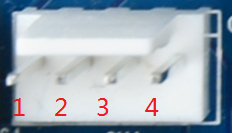
- CON1 to UART0, CON2 to UART1, CON3 to UART2, CON4 to UART3, The pin closest to the Ethernet is Pin1
Pin# 1 2 3 4 5 6 CON1,CON3,CON4 TXD RXD VDD_5V DGND CON2 RTS CTS TXD RXD DGND VDD_5V
- Note: UART0 and UART3 are brought to DB9 male connectors via RS232 conversion. COM0 is brought to UART0 and COM3 is brought to UART3
- LCD Interface Pin Spec
Smart4418 Pin# Name Description 1, 2 VDD_5V 5V output, can be used to power LCD 11,20,29, 45 DGND Ground 3-10 Blue LSB to MSB RGB blue 12-19 Green LSB to MSB RGB green 21-28 Red LSB to MSB RGB red 30 GPIOC13/PWM1 available for users 31 GPIOC15 occupied by FriendlyARM one wire technology to recognize LCD models,
and control backlight and implement resistive touch, not applicable for users.33 VDEN signal the external LCD that data is valid on the data bus 34 VSYNC vertical synchronization 35 HSYNC horizontal synchronization 36 LCDCLK LCD clock, Pixel frequency 41 I2C2_SCL I2C2 clock signal, for capacitive touch's data transmission 42 I2C2_SDA I2C2 data signal, for capacitive touch's data transmission 43 GPIOC16 interrupt pin for capacitive touch, used with I2C2 32,44 NC Not connected 37,38,39,40 NC For 40pin interface these 4 pins are NC 37,38,39,40 DGND For 45pin interface these 4 pins are DGND
Smart210 Pin# Name Description 1, 2 VDD_5V 5V output, can be used to power LCD 11,20,29, 45 DGND Ground 3-10 Blue LSB to MSB RGB blue 12-19 Green LSB to MSB RGB green 21-28 Red LSB to MSB RGB red 30 XpwmTOUT1 available for users 31 XEINT10 occupied by FriendlyARM one wire technology to recognize LCD models,
and control backlight and implement resistive touch, not applicable for users.33 VDEN signal the external LCD that data is valid on the data bus 34 VSYNC vertical synchronization 35 HSYNC horizontal synchronization 36 LCDCLK LCD clock, Pixel frequency 41 I2C2_SCL I2C2 clock signal, for capacitive touch's data transmission 42 I2C2_SDA I2C2 data signal, for capacitive touch's data transmission 43 XEINT14 interrupt pin for capacitive touch, used with I2C2 32,44 NC Not connected 37,38,39,40 NC For 40pin interface these 4 pins are NC 37,38,39,40 DGND For 45pin interface these 4 pins are DGND
- Power Port
- DC inlet, DC 4.0 * 1.7mm power adapter, voltage rage:4.7~5.6V
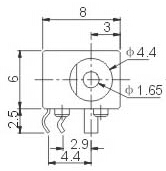

- 2.54mm pitch 2510-4P pinheader. Pin1~Pin4 are defined as: VDD_5V, DGND, DGND, 5V_IN
5V_IN is directly connected to DC power port. 5V_IN is the input to the switch and VDD_5V is the output of the switch
- 2.54mm pitch 2510-4P pinheader. Pin1~Pin4 are defined as: VDD_5V, DGND, DGND, 5V_IN

3.2 Board Dimension

- For more details please refer to the document:dxf file
4 Resources
- SDK schematics and hardware tech documents. These files are made based on the Smart210
- PCB Source File, please open with Allegro 16.5 or above
- PCB dxf file
- Schematic Source File, please open with OrCAD 16.5 or above
- schematic file in pdf version
- PCB Source File, please open with Allegro 16.5 or above
- Smart4418 CPU board software and hardware details
- Smart4418 schematic in pdf
5 Update Log
5.1 March-07-2016
- Released English version
5.2 March-08-2016
- Corrected a minor issue