Matrix - Analog to Digital Converter
Contents
1 Introduction
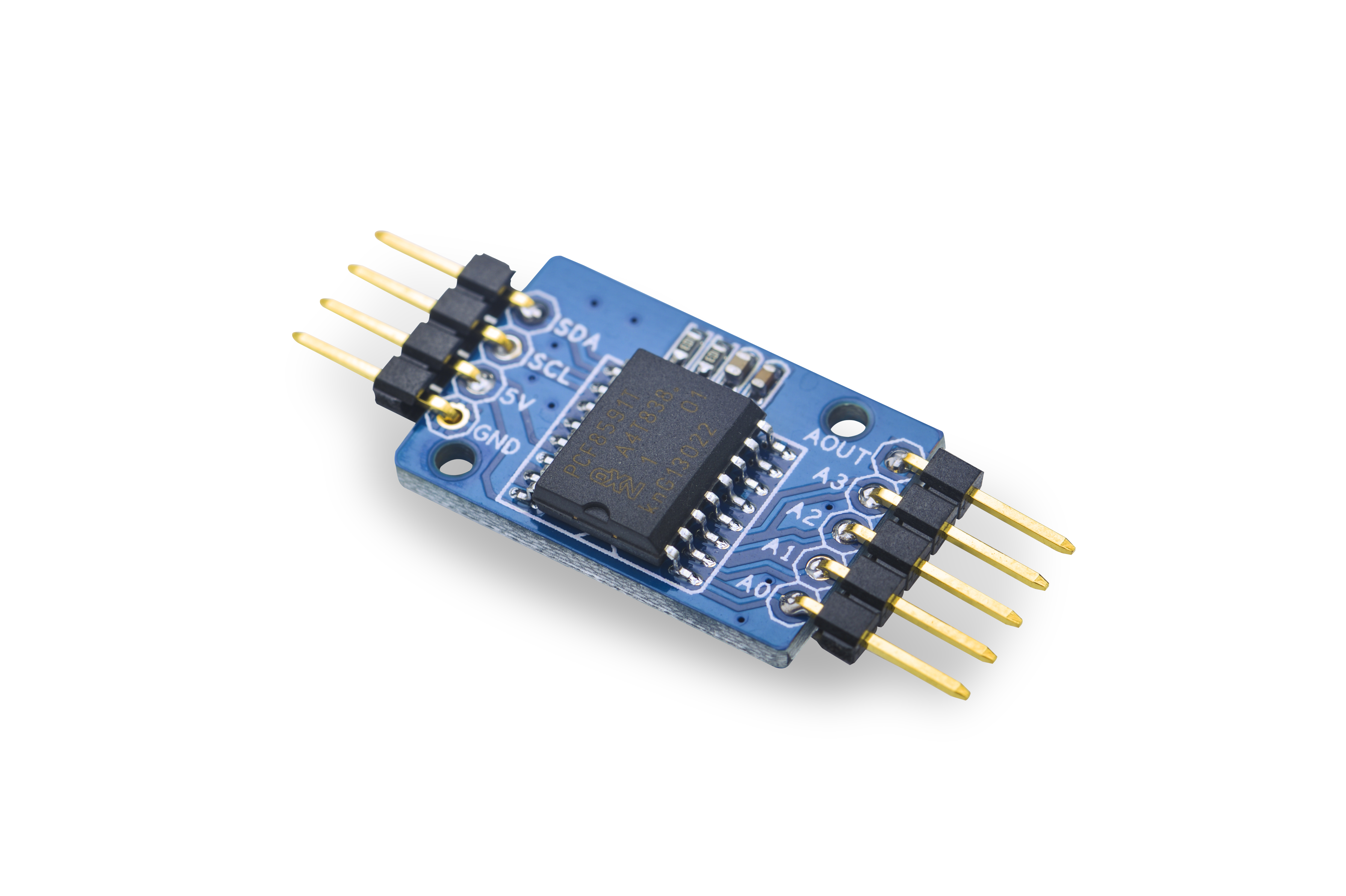
- The Matrix-Analog_to_Digital_Converter is a single-chip, single-supply low-power 8-bit CMOS data acquisition device.
- It utilizes the PCF8591 chip with four analog inputs, one analog output and a serial I2C-bus interface. Three address pins A0, A1 and A2 are used for programming the hardware address, allowing
the use of up to eight devices connected to the I2C-bus without additional hardware. Address, control and data to and from the device are transferred serially via the two-line bidirectional I2C-bus. The maximum conversion rate is given by the maximum speed of the I2C-bus.
- The I2C hardware address is configured to 1001000x
- The operating supply voltage is from 2.5V to 6.0V,Among the 2.54 mm spacing pin header the 5V pin is the supply voltage. If you need 0 - 3.3V analog signals and keep the acquisition resolution you can connect it to a 3.3V supply voltage.
2 Features
- Wide range supply voltage: 2.5V - 6.0V
- I2C interface: 3.3V/5V
- 8-bit A/D x 4
- 8-bit D/A x 1
- Small and easy to be used in various situations
- 2.54 mm spacing pin
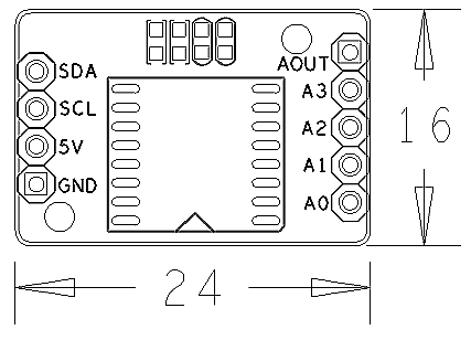
- PCB dimension (mm): 16 x 24
- Pin Description:
| Pin | Description |
| SDA | I2C SDA |
| SCL | I2C SCL |
| 5V | Supply Voltage 5V |
| GND | Ground |
| AOUT | Analog Output |
| A3 | Analog Input3 |
| A2 | Analog Input2 |
| A1 | Analog Input1 |
| A0 | Analog Input0 |
3 Basic Device Operation
The PCF8591's I2C-bus is for bidirectional, two-line communication between different ICs or modules. The two lines are a Serial DAta line (SDA) and a Serial CLock line (SCL). Both lines must
be connected to a positive supply via a pull-up resistor. Data transfer may be initiated only when the bus is not busy. The AINT0 - AINT4 pins are analog inputs which can be configured to single-ended or differential inputs. The supply voltage is 0 - VDD.
1. Each PCF8591 device in an I2C-bus system is activated by sending a valid address to the device. The address consists of a fixed part and a programmable part. The programmable part must be set according to the address pins A0, A1 and A2. The address is always sent as the first byte after the start condition in the I2C-bus protocol. The last bit of the address byte is the read/write-bit which sets the direction of the following data transfer.
2. The second byte sent to a PCF8591 device is stored in its control register and is required to control the device function. The upper nibble of the control register is used for enabling the analog output, and for programming the analog inputs as single-ended or differential inputs. The lower nibble selects one of the analog input channels defined by the upper nibble.
3. The on-chip D/A converter and a high-gain comparator are used temporarily during an A/D conversion cycle. An A/D conversion cycle is always started after sending a valid read mode address to a PCF8591 device. The A/D conversion cycle is triggered at the trailing edge of the acknowledge clock pulse and is executed while transmitting the result of the previous conversion。
4 Applications
4.1 Connect to NanoPi M1
Refer to the following connection diagram to connect the module to the NanoPi M1
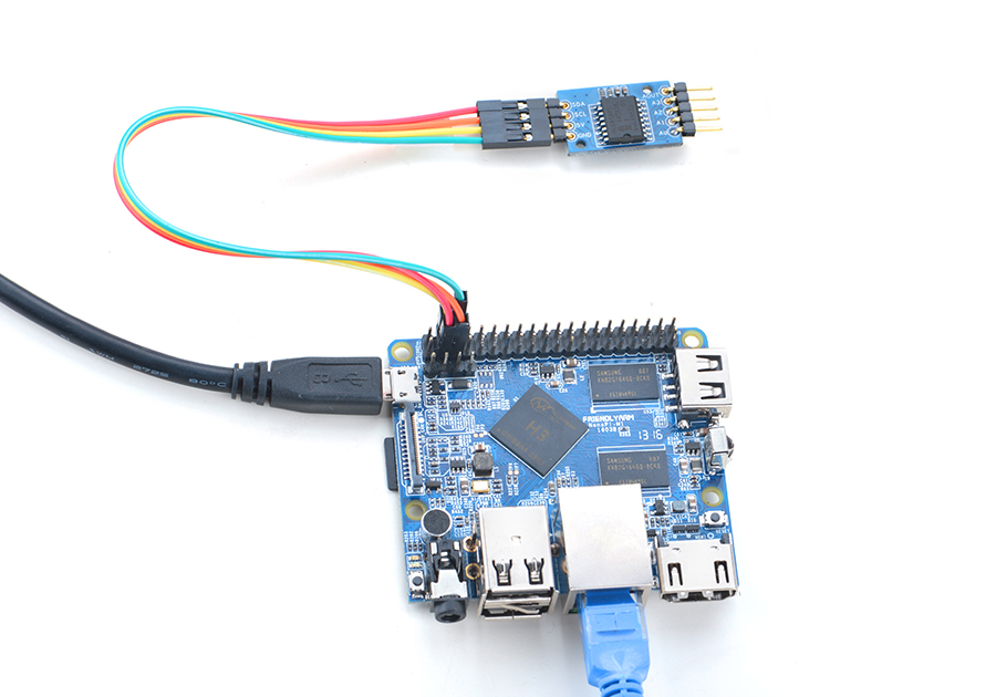
Connection Details:
| Matrix-Analog_to_Digital_Converter | NanoPi M1 |
| SDA | Pin3 |
| SCL | Pin5 |
| 5V | Pin4 |
| GND | Pin6 |
4.2 Connect to NanoPi 2
Refer to the following connection diagram to connect the module to the NanoPi 2:
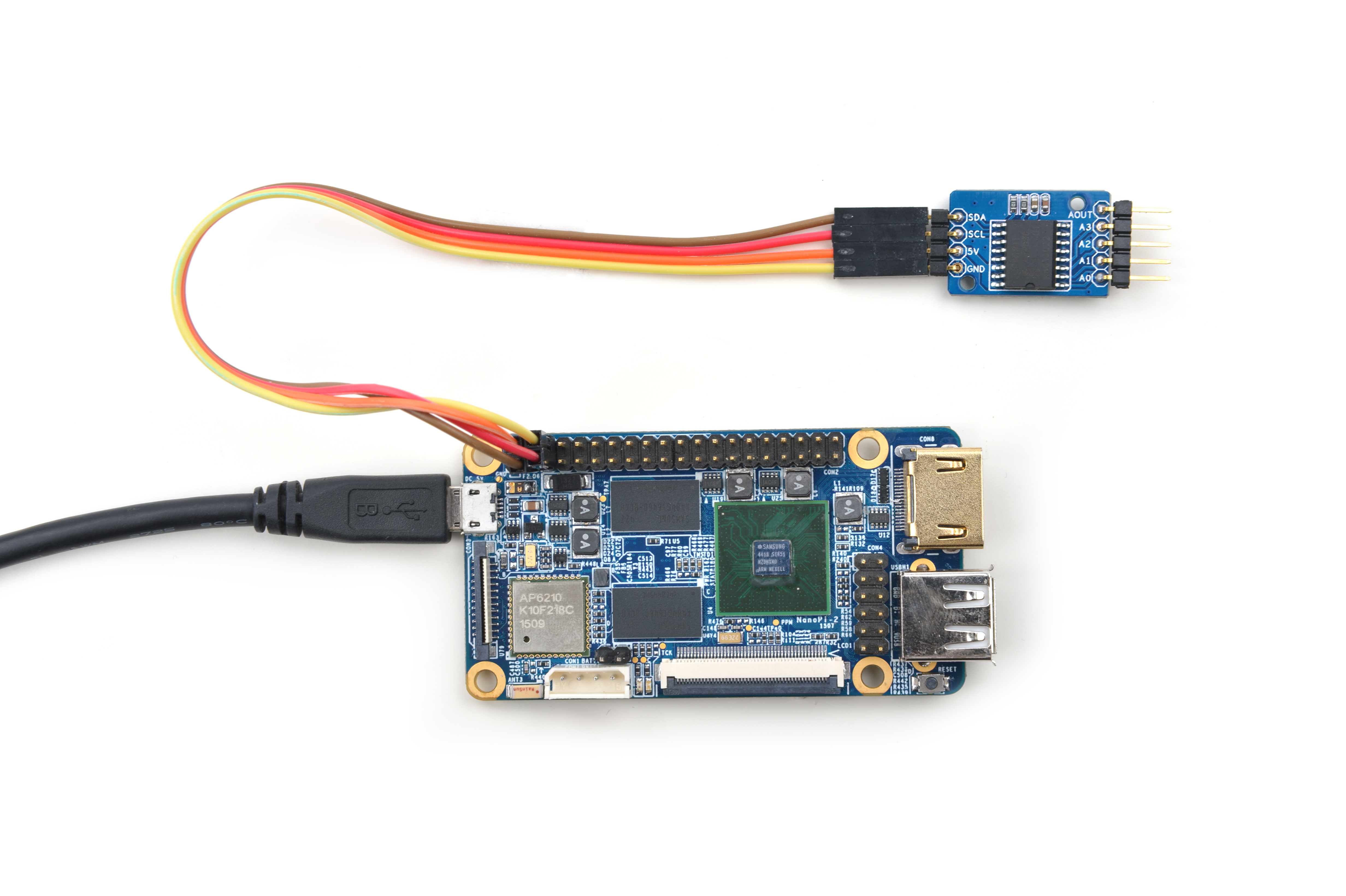
Connection Details:
| Matrix-Analog_to_Digital_Converter | NanoPi 2 |
| SDA | Pin3 |
| SCL | Pin5 |
| 5V | Pin4 |
| GND | Pin6 |
4.3 Connect to NanoPi M2 / NanoPi 2 Fire
Refer to the following connection diagram to connect the module to the NanoPi M2/ NanoPi 2 Fire:
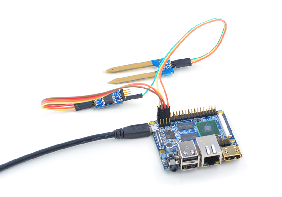
Connection Details:
| Matrix-Analog_to_Digital_Converter | NanoPi M2 |
| SDA | Pin3 |
| SCL | Pin5 |
| 5V | Pin4 |
| GND | Pin6 |
4.4 Connect to NanoPC-T2
Refer to the following connection diagram to connect the module to the NanoPC-T2
Matrix-Analog_to_Digital_Converter_NanoPC-T2
Connection Details:
| Matrix-Analog_to_Digital_Converter | NanoPC-T2 |
| SDA | Pin6 |
| SCL | Pin5 |
| 5V | Pin29 |
| GND | Pin30 |
5 Compile & Run Test Program
Boot your ARM board with Debian and copy the matrix code:
$ apt-get update && apt-get install git
$ git clone https://github.com/friendlyarm/matrix.git
If your cloning is done successfully a "matrix" directory will be generated.
Compile and install Matrix:
$ cd matrix
$ make && make install
Run test program:
$ matrix-adcNote: this module is not plug and play therefore before running the module please make sure it is connected to an ARM board.
Here is what you should observe:
The channel0 value is 2460When Channel 0 is connected to 5V its value reaches the maximum: 2550. When it is grounded its value is 0.
6 Code Sample
This Matrix code sample can work with all the ARM boards mentioned in this module's wiki. The name of this code sample is "matrix-analog_to_digital_converter". Here is its source code:
int main(int argc, char ** argv)
{
    int i = 0;
    int value = 0;
    int channel = 0;

    if (boardInit() < 0) {
        printf("Fail to init board\n");
        return -1;
    }

    if (argc == 2)
        channel = atoi(argv[1]);
    system("modprobe "DRIVER_MODULE);
    signal(SIGINT, intHandler);
    for (i=0; i<ADC_READ_TIMES; i++) {
        if (pcf8591Read(channel, &value) != -1) {
            printf("The channel%d value is %d\n", channel, value);
        } else {
            printf("Fail to get channel%d value\n", channel);
        }
    }
    system("rmmod "DRIVER_MODULE);

    return 0;
}
For more details about this APIs called in this code sample refer to Matrix API reference manual
7 Resources
8 Update Log
8.1 Feb-19-2016
- Added Section 5
8.2 June-17-2016
- Re-organized and simplified wiki
