Difference between revisions of "NanoPi R5S"
From FriendlyELEC WiKi
(→Hardware Spec) |
(→Hardware Spec) |
||
| Line 26: | Line 26: | ||
* GPIO: | * GPIO: | ||
** 12-pin 0.5mm FPC connector | ** 12-pin 0.5mm FPC connector | ||
| − | ** with up to 1x SPI, up to 3x UARTs, up to | + | ** with up to 1x SPI, up to 3x UARTs, up to 4x PWMs, up to 8x GPIOs |
* SD/MMC/SDIO/I2S: | * SD/MMC/SDIO/I2S: | ||
** 2x8-pin 1.27mm connector | ** 2x8-pin 1.27mm connector | ||
Revision as of 06:46, 6 May 2022
Contents
1 Introduction
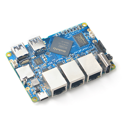
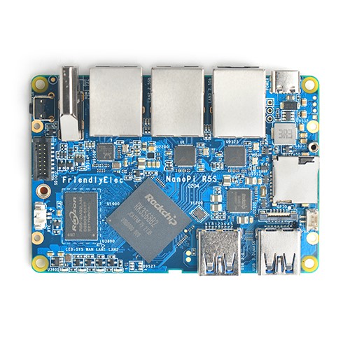
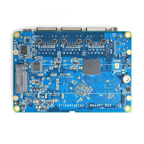
- The NanoPi R5S is a RK3568 SoC based ARM board.
2 Hardware Spec
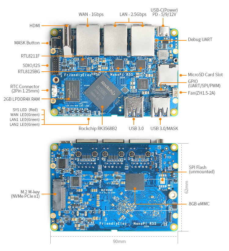
- SoC: Rockchip RK3568
- CPU: Quad-core ARM Cortex-A55 CPU, up to 2.0GHz
- GPU: Mali-G52 1-Core-2EE,supports OpenGL ES 1.1, 2.0, and 3.2, Vulkan 1.0 and 1.1, OpenCL 2.0 Full Profile
- VPU: 4KP60 H.265/H.264/VP9 video decoder, 1080P60 H.264/H.265 video encoder
- NPU: Support 0.8T
- RAM: 2GB LPDDR4X
- Flash: 8GB eMMC
- Ethernet: one Native Gigabit Ethernet, and two PCIe 2.5G Ethernet
- USB: two USB 3.0 Type-A ports
- HDMI:
- support HDMI1.4 and HDMI2.0 operation
- support up to 10 bits Deep Color modes
- support up to 1080p@120Hz and 4096x2304@60Hz
- support 3-D video formats
- PCIe: M.2 Key M, PCIe2.0 x1, support NVME, PCIe WiFi etc
- microSD: support UHS-I
- GPIO:
- 12-pin 0.5mm FPC connector
- with up to 1x SPI, up to 3x UARTs, up to 4x PWMs, up to 8x GPIOs
- SD/MMC/SDIO/I2S:
- 2x8-pin 1.27mm connector
- Compatible with SDIO3.0 protocol
- Compatible with SD3.0, MMC ver4.51
- 4bits data bus widths
- 1x I2S with 2x SDO and 3x SDI
- Debug: one Debug UART, 3 Pin 2.54mm header, 3.3V level, 1500000bps
- LEDs: 4 x GPIO Controlled LED (SYS, WAN, LAN1, LAN2)
- others:
- 2 Pin 1.27/1.25mm RTC battery input connector for low power RTC IC HYM8563TS
- MASK KEY for eMMC update
- one 5V Fan connector
- Power supply: USB-C, support PD, 5V/9V/12V input
- PCB: 8 Layer, 62x90x1.6mm
- Ambient Operating Temperature: 0℃ to 70℃
3 Diagram, Layout and Dimension
3.1 Layout
- 12-pin GPIO
Pin# GPIO SPI UART PWM POWER Description 1 VCC3V3_SYS 3.3V power output 2 VCC3V3_SYS 3.3V power output 3 GPIO3_C3 SPI1_CLK_M1 UART5_RX_M1 3.3V level 4 GND 5 GPIO3_C2 SPI1_MISOI_M1 UART5_TX_M1 3.3V level 6 GPIO3_A1 SPI1_CS0_M1 3.3V level 7 GPIO3_C1 SPI1_MOSI_M1 3.3V level 8 GND 9 GPIO4_C5 UART9_TX_M1 3.3V level 10 GPIO4_C6 UART9_RX_M1 3.3V level 11 GPIO3_C4 UART7_TX_M1 PWM14_M0 3.3V level 12 GPIO3_C5 UART7_RX_M1 PWM15_IR_M0 3.3V level
- 2x8-pin SDIO/I2S
Pin# GPIO SD/MMC/SDIO I2S POWER Description 1 VCC5V0_SYS 5V power output 2 VCC5V0_SYS 5V power output 3 GPIO3_C6 SDMMC2_D0_M0 I2S1_MCLK_M1 1.8V level 4 GPIO3_C7 SDMMC2_D1_M0 I2S1_SCLK_TX_M1 1.8V level 5 GND 6 GND 7 GPIO3_D0 SDMMC2_D2_M0 I2S1_LRCK_TX_M1 1.8V level 8 GPIO3_D3 SDMMC2_CLK_M0 I2S1_SDI1_M1 1.8V level 9 GND 10 GND 11 GPIO3_D1 SDMMC2_D3_M0 I2S1_SDO0_M1 1.8V level 12 GPIO3_D2 SDMMC2_CMD_M0 I2S1_SDI0_M1 1.8V level 13 GND 14 GND 15 GPIO3_D5 SDMMC2_PWREN_M0 I2S1_SDI3_M1 1.8V level 16 GPIO3_D4 SDMMC2_DET_M0 I2S1_SDI2_M1 1.8V level
- Debug UART Pin Spec
- 3.3V level signals, 1500000bps
Pin# Assignment Description 1 GND 0V 2 UART2DBG_TX output 3 UART2DBG_RX intput
- USB Port
- Each USB 3.0 port has 1.4A overcurrent protection.
- RTC
- RTC backup current is 0.25μA TYP (VDD =3.0V, TA =25℃).
- Connector P/N: Molex 53398-0271
4 Get Started
5 Link to Rockchip Resources
6 Schematic, PCB CAD File
- Schematic: []
- PCB CAD File:[]


