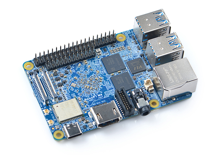
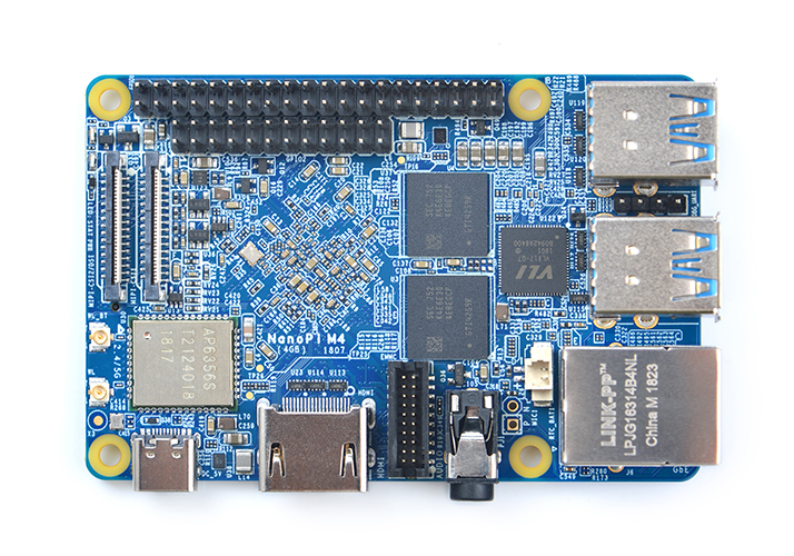
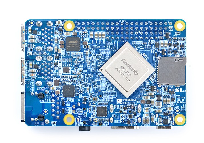
NanoPi M4
From FriendlyELEC WiKi
Revision as of 09:25, 21 August 2018 by Yonganch (Talk | contribs) (Created page with "查看中文 ==Introduction== Overview Front Back * * * =...")
Contents
1 Introduction
2 Hardware Spec
- SoC: Rockchip RK3399
- CPU: big.LITTLE,Dual-Core Cortex-A72(up to 2.0GHz) + Quad-Core Cortex-A53(up to 1.5GHz)
- GPU: Mali-T864 GPU,supports OpenGL ES1.1/2.0/3.0/3.1, OpenVG1.1, OpenCL, DX11, and AFBC
- VPU: 4K VP9 and 4K 10bits H265/H264 60fps decoding, Dual VOP, etc
- PMU: RK808-D PMIC, cooperated with independent DC/DC, enabling DVFS, solfware power-down, RTC wake-up, system sleep mode
- RAM: Dual-Channel 4GB LPDDR3-1866, or Dual-Channel 2GB DDR3-1866
- Flash: no Onboard eMMC, but has a eMMC socket
- Ethernet: Native Gigabit Ethernet
- Wi-Fi/BT: 802.11a/b/g/n/ac, Bluetooth 4.1, Wi-Fi and Bluetooth combo module, dual antenna interface
- Video Input: one or two 4-Lane MIPI-CSI, dual ISP, up to 13MPix/s,supports simultaneous input of dual camera data
- Video output
- HDMI: HDMI 2.0a, supports 4K@60Hz,HDCP 1.4/2.2
- one 4-Lane MIPI-DSI
- Audio Out: 3.5mm Dual channel headphone jack, or HDMI
- Audio In: one microphone input interface
- USB 3.0: four USB 3.0 Type-A ports
- USB Type-C: Supports USB2.0 OTG and Power input
- microSD Slot x 1
- 40Pin GPIO Extension ports:
- 3 X 3V/1.8V I2C, up to 1 x 3V UART, 1 X 3V SPI, 1 x SPDIF_TX, up to 8 x 3V GPIOs
- 1 x 1.8V 8 channels I2S
- 24Pin Extension ports:
- 2 independent native USB 2.0 Host interfaces
- PCIe x2
- PWM x1, PowerKey
- Debug: one Debug UART, 4 Pin 2.54mm header, 3V level, 1500000bps
- LED: 1 x power LED and 1 x GPIO Controlled LED
- RTC Battery: 2 Pin 1.27/1.25mm RTC battery input connector
- Power supply: DC 5V/3A
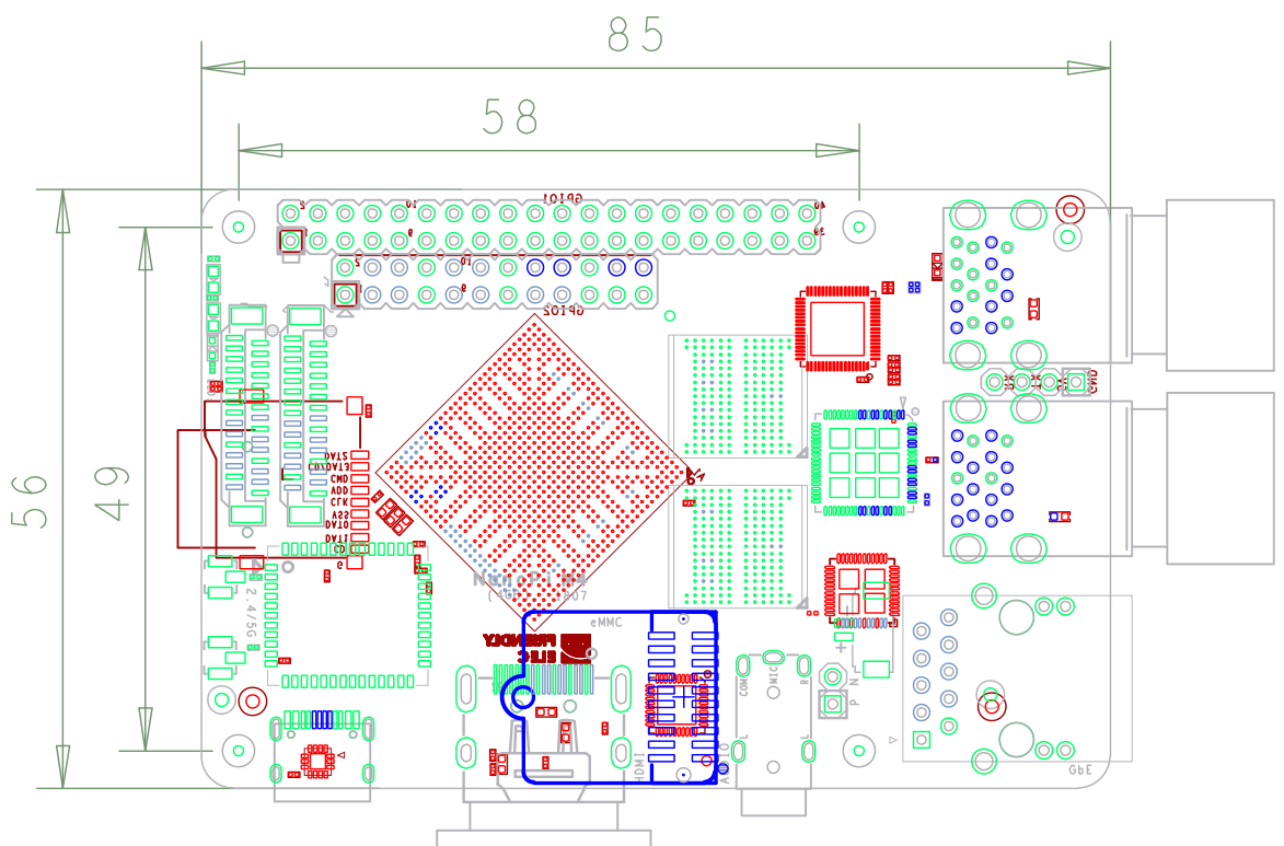
- PCB: 8 Layer, 85 mm x 56 mm
- Ambient Operating Temperature: 0℃ to 80℃
3 Diagram, Layout and Dimension
3.1 Layout
File:NanoPi M4-1807-IF-01.jpg
NanoPi M4 Layout
- 40 Pin GPIO1 Pin Spec
Pin# Assignment Pin# Assignment 1 VCC3V3_SYS 2 VDD_5V 3 I2C2_SDA(3V) 4 VDD_5V 5 I2C2_SCL(3V) 6 GND 7 GPIO1_A0(3V) 8 GPIO4_C1/I2C3_SCL(3V) 9 GND 10 GPIO4_C0/I2C3_SDA(3V) 11 GPIO1_A1(3V) 12 GPIO1_C2(3V) 13 GPIO1_A3(3V) 14 GND 15 GPIO1_A4(3V) 16 GPIO1_C6(3V) 17 VCC3V3_SYS 18 GPIO1_C7(3V) 19 SPI1_TXD/UARM4_TX(3V) 20 GND 21 SPI1_RXD/UARM4_RX(3V) 22 GPIO1_D0(3V) 23 SPI1_CLK(3V) 24 SPI1_CSn0(3V) 25 GND 26 GPIO4_C5/SPDIF_TX(3V) 27 I2C2_SDA(1.8V) 28 I2C2_SCL(1.8V) 29 I2S0_LRCK_RX(1.8V) 30 GND 31 I2S0_LRCK_TX(1.8V) 32 I2S_CLK(1.8V) 33 I2S0_SCLK(1.8V) 34 GND 35 I2S0_SDI0(1.8V) 36 I2S0_SDO0(1.8V) 37 I2S0_SDI1SDO3(1.8V) 38 I2S0_SDI2SDO2(1.8V) 39 GND 40 I2S0_SDI3SDO1(1.8V)
- 24 Pin GPIO2 Pin Spec
Pin# Assignment Pin# Assignment 1 VCC5V0_SYS 2 VCC5V0_SYS 3 PCIE_RX1_P 4 PCIE_TX1P 5 PCIE_RX1_N 6 PCIE_TX1N 7 GND 8 GND 9 PCIE_RX0_P 10 PCIE_TX0P 11 PCIE_RX0_N 12 PCIE_TX0N 13 GND 14 GND 15 PCIE_REF_CLKP 16 HOST0_DM 17 PCIE_REF_CLKN 18 HOST0_DP 19 GND 20 GND 21 PWR_KEY 22 HOST1_DM 23 GPIO4_C6/PWM1(3V) 24 HOST1_DP
- MIPI-CSI Interface Pin Spec
- 0.5mm FPC Connector
- MIPI-CSI2 can be configured to MIPI-DSI
Pin# MIPI-CSI1 MIPI-CSI2 Description 1 VCC5V0_SYS VCC5V0_SYS 5V Power ouput 2 VCC5V0_SYS VCC5V0_SYS 5V Power ouput 3 GND GND Return current path 4 VCC_CSI_AF2.8V VCC_CSI_AF2.8V 2.8V Power for VCM 5 VCC_CSI_1.2V VCC_CSI_1.2V 1.2V Power for image sensor core circuit 6 VCC1V8_CAM VCC1V8_CAM 1.8V power for I/O circuit 7 VCC_CSI_2.8V VCC_CSI_2.8V 2.8V power for image sensor analog circuit 8 VCC_CSI_1.0V VCC_CSI_1.0V 1.0V Power for image sensor core circuit 9 I2C1_SCL I2C2_SCL 1.8V I2C clock signal 10 I2C1_SDA I2C2_SDA 1.8V I2C data signal 11 MIPI_CSI0_RST MIPI_CSI1_RST reset camera module 12 MIPI_CSI0_PWN MIPI_CSI1_PWN Power down camera module 13 GND GND Return current path 14 GPIO2_B3_CIF_CLKOUTA GPIO2_B3_CIF_CLKOUTA MCLK to camera module 15 GND GND Return current path 16 MIPI_RX0_D3P MIPI_TX1/RX1_D3P MIPI CSI positive differential data line transceiver output 17 MIPI_RX0_D3N MIPI_TX1/RX1_D3N MIPI CSI negative differential data line transceiver output 18 GND GND Return current path 19 MIPI_RX0_D2P MIPI_TX1/RX1_D2P MIPI CSI positive differential data line transceiver output 20 MIPI_RX0_D2N MIPI_TX1/RX1_D2N MIPI CSI negative differential data line transceiver output 21 GND GND Return current path 22 MIPI_RX0_D1P MIPI_TX1/RX1_D1P MIPI CSI positive differential data line transceiver output 23 MIPI_RX0_D1N MIPI_TX1/RX1_D1N MIPI CSI negative differential data line transceiver output 24 GND GND Return current path 25 MIPI_RX0_CLKP MIPI_TX1/RX1_CLKP MIPI CSI positive differential clock line transceiver output 26 MIPI_RX0_CLKN MIPI_TX1/RX1_CLKN MIPI CSI negative differential clock line transceiver output 27 GND GND Return current path 28 MIPI_RX0_D0P MIPI_TX1/RX1_D0P MIPI CSI positive differential data line transceiver output 29 MIPI_RX0_D0N MIPI_TX1/RX1_D0N MIPI CSI negative differential data line transceiver output 30 GND GND Return current path
- Debug UART Pin Spec
- 3V level signals, 1500000bps
Pin# Assignment Description 1 GND 0V 2 VCC5V0_SYS 5V power output 3 UART2DBG_TX output 4 UART2DBG_RX intput
- USB Port
- USB 3.0 port has 2A overcurrent protection.
- RTC
- RTC backup current is 27uA.
- Connector P/N: Molex 53398-0271
- Notes
- Power Input : 5V/3A, via USB Type-C or Pin2&Pin4 of the 40 Pin GPIO1 header
- For more details refer to the Schematic: M4-1807-Schematic.pdf NanoPi M4-1807-Schematic.pdf
3.2 Board Dimension
- For more details refer to the CAD document: M4_1807_Drawing%28dxf%29.zip NanoPi M4_1807_Drawing(dxf).zip
4 Link to Rockchip Resources
- Link to Rockchip's resources: https://gitlab.com/friendlyelec/rk3399-nougat/tree/NanoPi M4-nougat/RKDocs
- RK3399 datasheet V1.6
- RK3399TRM V1.4
5 Schematic, PCB CAD File
- Schematic: M4-1807-Schematic.pdf NanoPi M4-1807-Schematic.pdf
- PCB CAD File:M4_1807_Drawing%28dxf%29.zip NanoPi M4_1807_Drawing(dxf).zip


