Difference between revisions of "All-in-One Android Touch Screen"
From FriendlyELEC WiKi
(Created page with "查看中文 ==Introduction==") |
(→Resources) |
||
| (28 intermediate revisions by 2 users not shown) | |||
| Line 2: | Line 2: | ||
==Introduction== | ==Introduction== | ||
| + | [[File:9inch_All-in-One_Android_Touch_Display-1.png|thumb|]] | ||
| + | [[File:9inch_All-in-One_Android_Touch_Display-2.png|thumb|]] | ||
| + | [[File:9inch_All-in-One_Android_Touch_Display-5.png|thumb|]] | ||
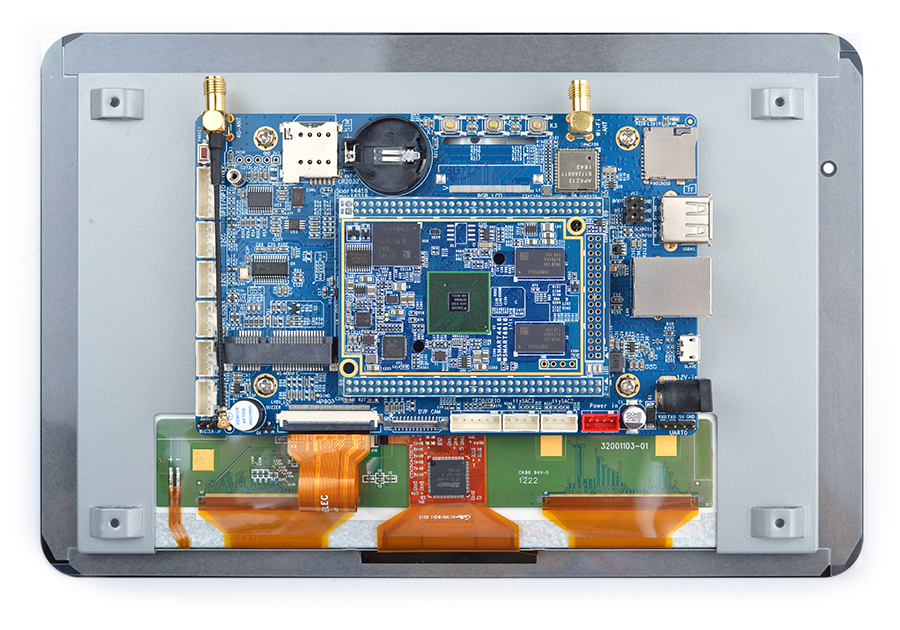
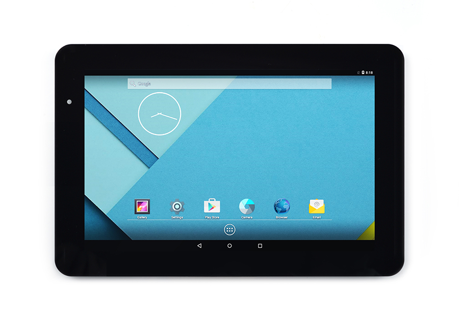
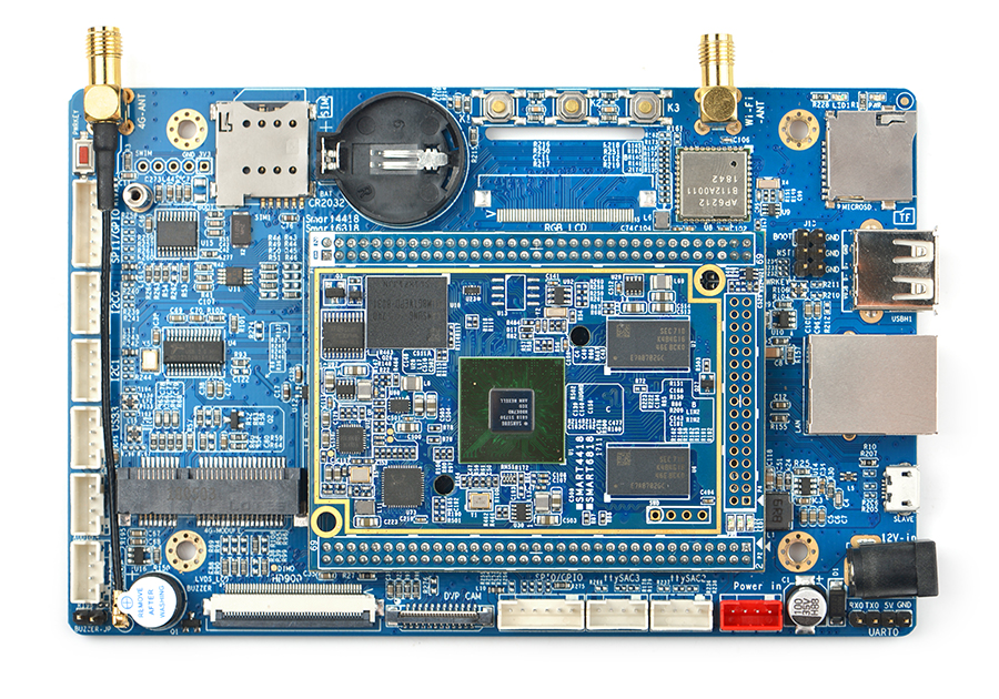
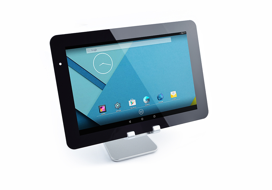
| + | * All-in-One Android Touch Screen is designed and developed by FriendlyElec. It is a comprehensive solution with a 9" HD LCD and capacitive touch panel. It is based on FriendlyElec's Smart6818 CPU board which uses Samsung's octa-core Cortex-A53 S5P6818. Its frequency can scale up to 1.4Ghz. It has 1GB DDR3 RAM and 8GB eMMC flash.It has a power management unit which implements software power on/off and hardware wake-up functions.It integrates Wi-Fi, bluetooth, Gbps Ethernet and audio. It supports EC20 4G modules.Its display resolution is 1280 x 800. It has a capacitive touch panel. Its back-light is controllable via i2c. In addition it has popular interfaces such as I2C, SPI, RS232-UART, USB etc.These features make it a good platform for fast prototyping and industrial applications. | ||
| + | |||
| + | ==Hardware Spec== | ||
| + | [[File:All-in-One Android Touch Screen-1.jpg|thumb|550px|Features]] | ||
| + | * SoC: Samsung Octa-Core Cortex-A53 S5P6818 | ||
| + | * Clock: Dynamic scaling from 400Mhz up to 1.4GHz | ||
| + | * DDR3 RAM: 1GB | ||
| + | * eMMC: 8GB | ||
| + | * Network: 1000/100/10M Ethernet(RTL8211E) with unique MAC address | ||
| + | * Wi-Fi/Bluetooth: onboard Wi-Fi Bluetooth (AP6212) with SMA antenna interface | ||
| + | * 4G: it works with EC20 4G modules via MiniPCIe interface. It supports only data service, no voice service. Onboard IPX to SMA interface available | ||
| + | * SIM Card Slot: pop-up MicroSIM card slot | ||
| + | * DVP Camera Interface: 24pin 0.5mm pitch FPC seat | ||
| + | * I2C: 2 x I2C interface, 2.0mm pitch PH-4A connector | ||
| + | * SPI/GPIO: 2 x SPI interface(SPI0,SPI1), 2.0mm pitch PH-6A connector. They can be used as GPIOs | ||
| + | * TTL Serial: 1 x 3-wire serial interface(UART0), 2.54mm pitch | ||
| + | * RS-232 Serial Port: 2 x 3-wire serial interface(UART3), 2.0mm pitch PH-4A connector | ||
| + | * USB Host: x 3, extended from a USB 2.0 hub (compatible with USB 1.1)<br />1 x USB Type A interface,2 x 2.0mm pitch PH-4A connector | ||
| + | * USB Slave: x 1, MicroUSB, It only supports data transmission. | ||
| + | * Audio Input/Output: it supports audio recording and playing. 2.0mm pitch PH-4A connector | ||
| + | * Key: PWRKEY(power key), K1/K2/K3 programmable keys | ||
| + | * RTC Battery Seat: Onboard RTC battery seat(CR2032 battery) | ||
| + | * Buzzer: 1 x PWM buzzer. You need to short the buzzer pins with a jumper to enable it | ||
| + | * Other Resources: Onboard one 3-Axis Digital Accelerometer, one 3 x 2Pin 2.54mm pitch pin-header(including a pin for boot options: eMMC or MicroSD card. When it is set HIGH it will boot from eMMC otherwise boot from MicroSD), one RST, one PWRKEY and three GNDs | ||
| + | * Power Supply: DC 9V~15V/2A | ||
| + | * Dimension: 235.12 x 156.4(mm) | ||
| + | |||
| + | ==Board Dimension== | ||
| + | [[File:9inch_All-in-One_Android_Touch_Display-pcb.png|frameless|500px|]] | ||
| + | * Schematic:[[http://wiki.friendlyarm.com/wiki/images/2/24/9inch_All-in-One_Android_Touch_Display_1901.pdf All-in-One Android Touch Screen schematic file in pdf format)]] | ||
| + | * Schematic:[[http://wiki.friendlyarm.com/wiki/index.php/File:9inch_All-in-One_Android_Touch_Display-Schematic.rar All-in-One Android Touch Screen schematic file,Capture 16.5 or above ]] | ||
| + | * PCB: [[http://wiki.friendlyarm.com/wiki/index.php/File:9inch_All-in-One_Android_Touch_Display_PCB-16.5.rar All-in-One Android Touch Screen PCB file,Allegro 16.5 or above ]] | ||
| + | * PCB dimension: [[http://wiki.friendlyarm.com/wiki/index.php/File:Dimension_9inch_All-in-One_Android_Touch_Display_PCB.rar All-in-One Android Touch Screen PCB dimension file in dxf format]] | ||
| + | * Datasheet: [[http://wiki.friendlyarm.com/wiki/images/d/de/9%E5%AF%B8-%E5%B8%A6TP-ED090NA-01D_Final_Ver01_20110805.pdf HD900 Specification in pdf format]] | ||
| + | |||
| + | ==Layout== | ||
| + | * '''HD900(LVDS) Pin Spec''' | ||
| + | ::{| class="wikitable" | ||
| + | |- | ||
| + | | style="background: PaleTurquoise; color: black" colspan="1"| '''Pin#''' || style="background: PaleTurquoise; color: black" colspan="1"| '''Symbol'''|| style="background: PaleTurquoise; color: black" colspan="1"| '''I/O'''|| style="background: PaleTurquoise; color: black" colspan="1"| '''Function''' | ||
| + | |- | ||
| + | |1 || VDD-C-TP || P ||Power supply input for C-TP | ||
| + | |- | ||
| + | |2 || GND-C-TP || P ||Ground for C-TP | ||
| + | |- | ||
| + | |3 || RST-C-TP || I ||Reset C-TP | ||
| + | |- | ||
| + | |4 || SCL || I || I2C Clock | ||
| + | |- | ||
| + | |5 || SDA ||I/O|| I2C Data | ||
| + | |- | ||
| + | |6 || INT || O || Interrupt pin | ||
| + | |- | ||
| + | |7 || GND || P || Ground | ||
| + | |- | ||
| + | |8 || GND || P || Ground | ||
| + | |- | ||
| + | |9 || GND || P || Ground | ||
| + | |- | ||
| + | |10 || VCOM || P || Common Voltage | ||
| + | |- | ||
| + | |11 || VDD || P ||Power Voltage for digital circuit | ||
| + | |- | ||
| + | |12 || VDD || P ||Power Voltage for digital circuit | ||
| + | |- | ||
| + | |13 || RST GLOBAL || I ||Global reset pin | ||
| + | |- | ||
| + | |14 || STBYB || I ||Standby mode | ||
| + | |- | ||
| + | |15 || GND || P ||Ground | ||
| + | |- | ||
| + | |16 || RXIN0- || I ||-LVDS differential data input | ||
| + | |- | ||
| + | |17 || RXIN0+ || I ||+LVDS differential data input | ||
| + | |- | ||
| + | |18 || GND || P ||Ground | ||
| + | |- | ||
| + | |19 || RXIN1- || I || -LVDS differential data input | ||
| + | |- | ||
| + | |20 || RXIN1+ || I || +LVDS differential data input | ||
| + | |- | ||
| + | |21 || GND || P ||Ground | ||
| + | |- | ||
| + | |22 || RXIN2- || I ||-LVDS differential data input | ||
| + | |- | ||
| + | |23 || RXIN2+ || I || +LVDS differential data input | ||
| + | |- | ||
| + | |24 || GND || P ||Ground | ||
| + | |- | ||
| + | |25 || RXCLKIN- || I ||-LVDS differential clock input | ||
| + | |- | ||
| + | |26 || RXCLKIN+ || I ||+LVDS differential clock input | ||
| + | |- | ||
| + | |27 || GND || P ||Ground | ||
| + | |- | ||
| + | |28 || RXIN3- || I ||-LVDS differential data input | ||
| + | |- | ||
| + | |29 || RXIN3+ || I ||+LVDS differential data input | ||
| + | |- | ||
| + | |30 || GND || P ||Ground | ||
| + | |- | ||
| + | |31 || GND || P ||Ground | ||
| + | |- | ||
| + | |32 || DIMO || O || Backlight CABC controller signal output | ||
| + | |- | ||
| + | |33 || SELB || I || 6/8bit mode select | ||
| + | |- | ||
| + | |34 || AVDD || P || Power for Analog Circuit | ||
| + | |- | ||
| + | |35 || GND || P || Ground | ||
| + | |- | ||
| + | |36 || LED- || P || LED Cathode | ||
| + | |- | ||
| + | |37 || LED- || P || LED Cathode | ||
| + | |- | ||
| + | |38 || L/R || I || Horiaontal inversion | ||
| + | |- | ||
| + | |39 || U/D || I || Vertiacl inversion | ||
| + | |- | ||
| + | |40 || VGL || P || Gate OFF Voltage | ||
| + | |- | ||
| + | |41 || CABCEN1 || I || CABC H/W enable | ||
| + | |- | ||
| + | |42 || CANCEN0 || I || CABC H/W enable | ||
| + | |- | ||
| + | |43 || VGH || P || Gate ON Voltage | ||
| + | |- | ||
| + | |44 || LED+ || P || LED Anode | ||
| + | |- | ||
| + | |45 || LED+ || P || LED Anode | ||
| + | |} | ||
| + | |||
| + | * '''DVP CAM Interface Pin Spec''' | ||
| + | ::{| class="wikitable" | ||
| + | |- | ||
| + | | style="background: PaleTurquoise; color: black" colspan="1"| '''Pin#''' || style="background: PaleTurquoise; color: black" colspan="1"| '''Name'''|| style="background: PaleTurquoise; color: black" colspan="1"| '''Function''' | ||
| + | |- | ||
| + | |1, 2 || SYS_3.3V || 3.3V power output, to camera modules | ||
| + | |- | ||
| + | |7,9,13,15,24 || GND || Gound, 0V | ||
| + | |- | ||
| + | |3 || I2C2_SCL || I2C Clock Signal | ||
| + | |- | ||
| + | |4 || I2C2_SDA || I2C Data Signal | ||
| + | |- | ||
| + | |5 || GPIOE15 || Regular GPIO, control signals output to camera modules | ||
| + | |- | ||
| + | |6 || GPIOE14 || Regular GPIO, control signals output to camera modules | ||
| + | |- | ||
| + | |8 || MCLK || Clock signals output to camera modules | ||
| + | |- | ||
| + | |10 || NC || Not Connected | ||
| + | |- | ||
| + | |11 || VSYNC || vertical synchronization to CPU from camera modules | ||
| + | |- | ||
| + | |12 || HREF/HSYNC || HREF/HSYNC signal to CPU from camera modules | ||
| + | |- | ||
| + | |14 || PCLK || PCLK signal to CPU from camera modules | ||
| + | |- | ||
| + | |16-23 || Data bit7-0 || data signals | ||
| + | |} | ||
| + | |||
| + | ==Hardware Setup== | ||
| + | *All-in-One Android Touch Screen has a BOOT pin-header which is used to set the system to boot from either TF card or eMMC: | ||
| + | ** BOOT not shorted---boot from eMMC | ||
| + | ** BOOT shorted by jumper---boot from TF card | ||
| + | Here is a hardware setup:<br /> | ||
| + | [[File:9inch_All-in-One_Android_Touch_Display-boot-en.png|frameless|500px|]] | ||
| + | * Connect HD900: | ||
| + | [[File:9inch_All-in-One_Android_Touch_Display-3.png|frameless|500px|]] | ||
| + | [[File:9inch_All-in-One_Android_Touch_Display-4.png|frameless|500px|]] | ||
| + | [[File:9inch_All-in-One_Android_Touch_Display-2.png|frameless|500px|]] | ||
| + | [[File:9inch_All-in-One_Android_Touch_Display.png|frameless|500px|]] | ||
| + | |||
| + | ==Resources== | ||
| + | * Schematic:[[http://wiki.friendlyarm.com/wiki/images/2/24/9inch_All-in-One_Android_Touch_Display_1901.pdf All-in-One Android Touch Screen schematic file in pdf format)]] | ||
| + | * Schematic:[[http://wiki.friendlyarm.com/wiki/index.php/File:9inch_All-in-One_Android_Touch_Display-Schematic.rar All-in-One Android Touch Screen schematic file,Capture 16.5 or above ]] | ||
| + | * PCB: [[http://wiki.friendlyarm.com/wiki/index.php/File:9inch_All-in-One_Android_Touch_Display_PCB-16.5.rar All-in-One Android Touch Screen PCB file,Allegro 16.5 or above ]] | ||
| + | * PCB dimension: [[http://wiki.friendlyarm.com/wiki/index.php/File:Dimension_9inch_All-in-One_Android_Touch_Display_PCB.rar All-in-One Android Touch Screen PCB dimension file in dxf format]] | ||
| + | * Datasheet: [[http://wiki.friendlyarm.com/wiki/images/d/de/9%E5%AF%B8-%E5%B8%A6TP-ED090NA-01D_Final_Ver01_20110805.pdf HD900 Specification in pdf format]] | ||
| + | |||
| + | ==Update Log== | ||
| + | ===April-2-2019=== | ||
| + | 1) Released English version | ||
| + | |||
| + | ===April-19-2019=== | ||
| + | 1) Updated section 5 | ||
Latest revision as of 07:23, 19 June 2019
Contents
1 Introduction
- All-in-One Android Touch Screen is designed and developed by FriendlyElec. It is a comprehensive solution with a 9" HD LCD and capacitive touch panel. It is based on FriendlyElec's Smart6818 CPU board which uses Samsung's octa-core Cortex-A53 S5P6818. Its frequency can scale up to 1.4Ghz. It has 1GB DDR3 RAM and 8GB eMMC flash.It has a power management unit which implements software power on/off and hardware wake-up functions.It integrates Wi-Fi, bluetooth, Gbps Ethernet and audio. It supports EC20 4G modules.Its display resolution is 1280 x 800. It has a capacitive touch panel. Its back-light is controllable via i2c. In addition it has popular interfaces such as I2C, SPI, RS232-UART, USB etc.These features make it a good platform for fast prototyping and industrial applications.
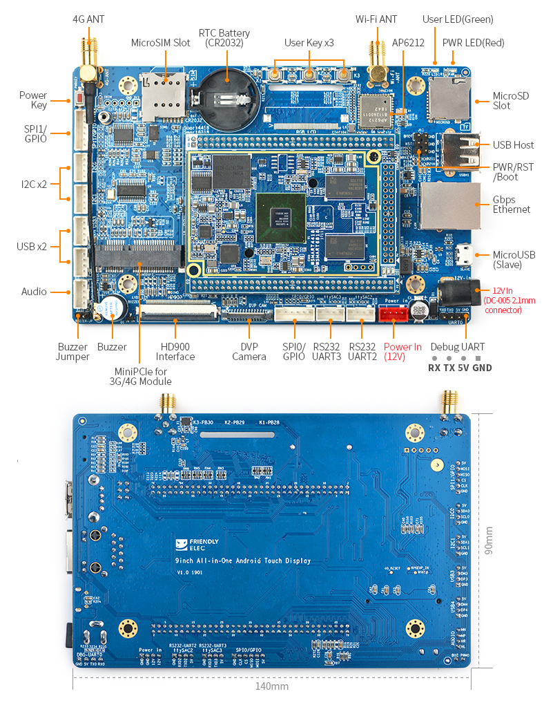
2 Hardware Spec
- SoC: Samsung Octa-Core Cortex-A53 S5P6818
- Clock: Dynamic scaling from 400Mhz up to 1.4GHz
- DDR3 RAM: 1GB
- eMMC: 8GB
- Network: 1000/100/10M Ethernet(RTL8211E) with unique MAC address
- Wi-Fi/Bluetooth: onboard Wi-Fi Bluetooth (AP6212) with SMA antenna interface
- 4G: it works with EC20 4G modules via MiniPCIe interface. It supports only data service, no voice service. Onboard IPX to SMA interface available
- SIM Card Slot: pop-up MicroSIM card slot
- DVP Camera Interface: 24pin 0.5mm pitch FPC seat
- I2C: 2 x I2C interface, 2.0mm pitch PH-4A connector
- SPI/GPIO: 2 x SPI interface(SPI0,SPI1), 2.0mm pitch PH-6A connector. They can be used as GPIOs
- TTL Serial: 1 x 3-wire serial interface(UART0), 2.54mm pitch
- RS-232 Serial Port: 2 x 3-wire serial interface(UART3), 2.0mm pitch PH-4A connector
- USB Host: x 3, extended from a USB 2.0 hub (compatible with USB 1.1)
1 x USB Type A interface,2 x 2.0mm pitch PH-4A connector - USB Slave: x 1, MicroUSB, It only supports data transmission.
- Audio Input/Output: it supports audio recording and playing. 2.0mm pitch PH-4A connector
- Key: PWRKEY(power key), K1/K2/K3 programmable keys
- RTC Battery Seat: Onboard RTC battery seat(CR2032 battery)
- Buzzer: 1 x PWM buzzer. You need to short the buzzer pins with a jumper to enable it
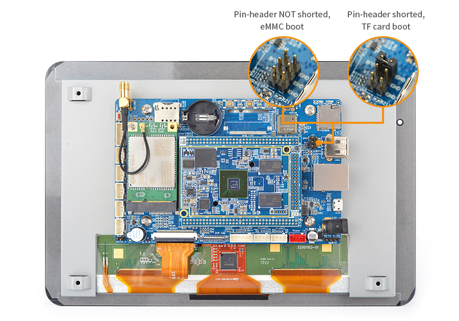
- Other Resources: Onboard one 3-Axis Digital Accelerometer, one 3 x 2Pin 2.54mm pitch pin-header(including a pin for boot options: eMMC or MicroSD card. When it is set HIGH it will boot from eMMC otherwise boot from MicroSD), one RST, one PWRKEY and three GNDs
- Power Supply: DC 9V~15V/2A
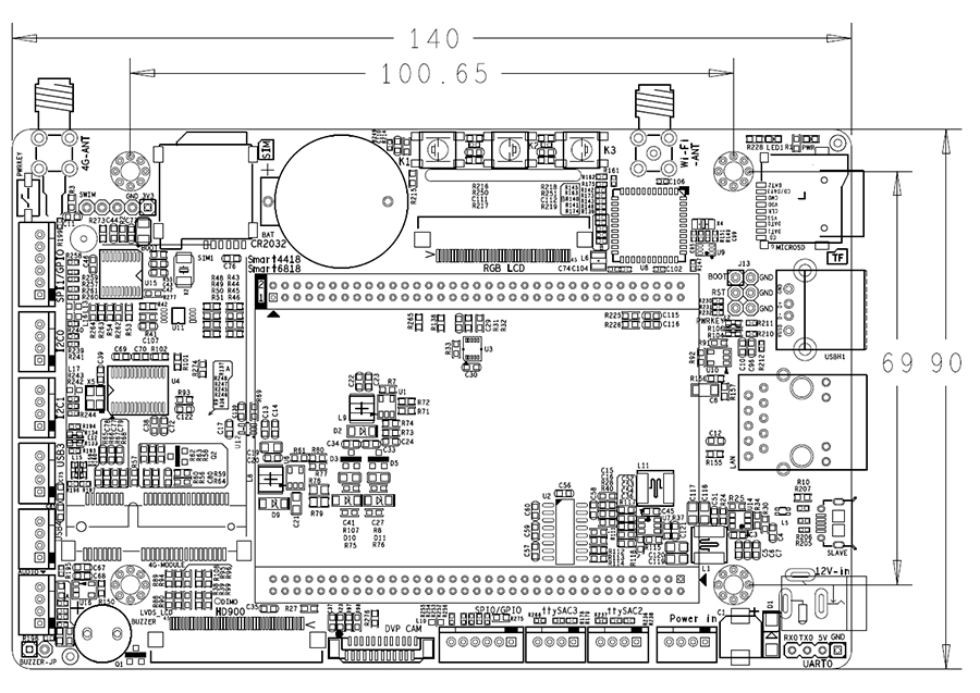
- Dimension: 235.12 x 156.4(mm)
3 Board Dimension
- Schematic:[All-in-One Android Touch Screen schematic file in pdf format)]
- Schematic:[All-in-One Android Touch Screen schematic file,Capture 16.5 or above ]
- PCB: [All-in-One Android Touch Screen PCB file,Allegro 16.5 or above ]
- PCB dimension: [All-in-One Android Touch Screen PCB dimension file in dxf format]
- Datasheet: [HD900 Specification in pdf format]
4 Layout
- HD900(LVDS) Pin Spec
Pin# Symbol I/O Function 1 VDD-C-TP P Power supply input for C-TP 2 GND-C-TP P Ground for C-TP 3 RST-C-TP I Reset C-TP 4 SCL I I2C Clock 5 SDA I/O I2C Data 6 INT O Interrupt pin 7 GND P Ground 8 GND P Ground 9 GND P Ground 10 VCOM P Common Voltage 11 VDD P Power Voltage for digital circuit 12 VDD P Power Voltage for digital circuit 13 RST GLOBAL I Global reset pin 14 STBYB I Standby mode 15 GND P Ground 16 RXIN0- I -LVDS differential data input 17 RXIN0+ I +LVDS differential data input 18 GND P Ground 19 RXIN1- I -LVDS differential data input 20 RXIN1+ I +LVDS differential data input 21 GND P Ground 22 RXIN2- I -LVDS differential data input 23 RXIN2+ I +LVDS differential data input 24 GND P Ground 25 RXCLKIN- I -LVDS differential clock input 26 RXCLKIN+ I +LVDS differential clock input 27 GND P Ground 28 RXIN3- I -LVDS differential data input 29 RXIN3+ I +LVDS differential data input 30 GND P Ground 31 GND P Ground 32 DIMO O Backlight CABC controller signal output 33 SELB I 6/8bit mode select 34 AVDD P Power for Analog Circuit 35 GND P Ground 36 LED- P LED Cathode 37 LED- P LED Cathode 38 L/R I Horiaontal inversion 39 U/D I Vertiacl inversion 40 VGL P Gate OFF Voltage 41 CABCEN1 I CABC H/W enable 42 CANCEN0 I CABC H/W enable 43 VGH P Gate ON Voltage 44 LED+ P LED Anode 45 LED+ P LED Anode
- DVP CAM Interface Pin Spec
Pin# Name Function 1, 2 SYS_3.3V 3.3V power output, to camera modules 7,9,13,15,24 GND Gound, 0V 3 I2C2_SCL I2C Clock Signal 4 I2C2_SDA I2C Data Signal 5 GPIOE15 Regular GPIO, control signals output to camera modules 6 GPIOE14 Regular GPIO, control signals output to camera modules 8 MCLK Clock signals output to camera modules 10 NC Not Connected 11 VSYNC vertical synchronization to CPU from camera modules 12 HREF/HSYNC HREF/HSYNC signal to CPU from camera modules 14 PCLK PCLK signal to CPU from camera modules 16-23 Data bit7-0 data signals
5 Hardware Setup
- All-in-One Android Touch Screen has a BOOT pin-header which is used to set the system to boot from either TF card or eMMC:
- BOOT not shorted---boot from eMMC
- BOOT shorted by jumper---boot from TF card
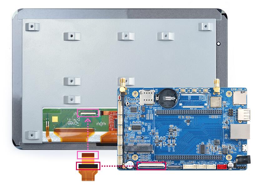
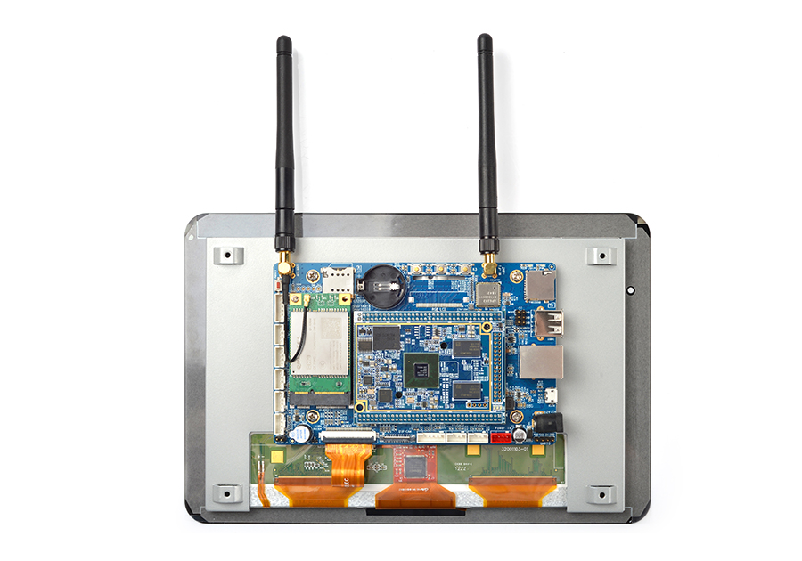
- Connect HD900:
6 Resources
- Schematic:[All-in-One Android Touch Screen schematic file in pdf format)]
- Schematic:[All-in-One Android Touch Screen schematic file,Capture 16.5 or above ]
- PCB: [All-in-One Android Touch Screen PCB file,Allegro 16.5 or above ]
- PCB dimension: [All-in-One Android Touch Screen PCB dimension file in dxf format]
- Datasheet: [HD900 Specification in pdf format]
7 Update Log
7.1 April-2-2019
1) Released English version
7.2 April-19-2019
1) Updated section 5
