SOM-RK3399
From FriendlyELEC WiKi
Contents
1 Introduction
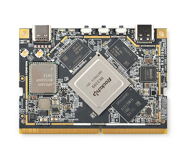
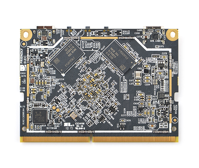
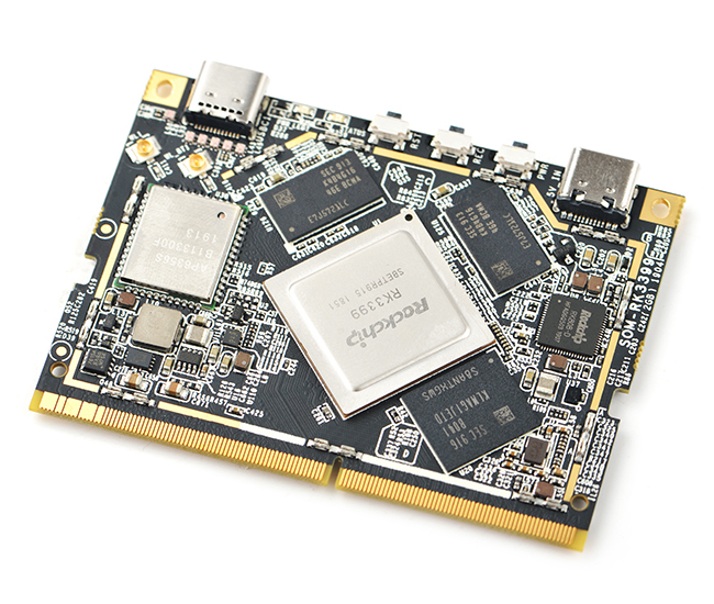
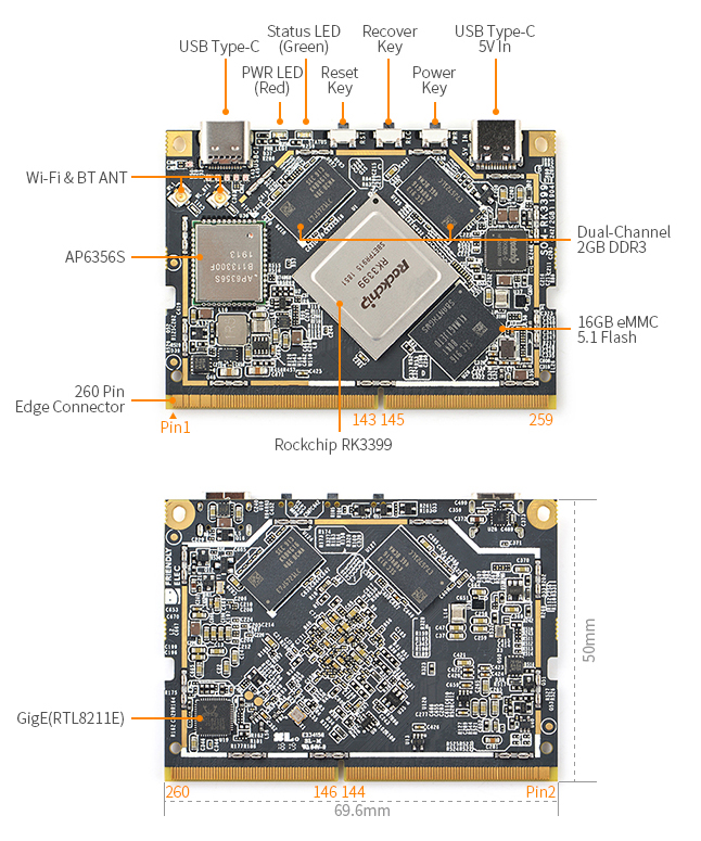
- The SOM-RK3399 is a 260-pin high performance ARM module designed and developed by FriendlyElec. It is based on Rockchip’s 64-bit hexa-core RK3399 SoC. The regular version has 2GB DDR3 RAM, 16GB Flash, onboard 2x2 MIMO dual-antenna WiFi module. Its dimension is 69.6 x 50 mm. It has a TypeC power port and USB-C display port, and can work by itself without a carrier board.
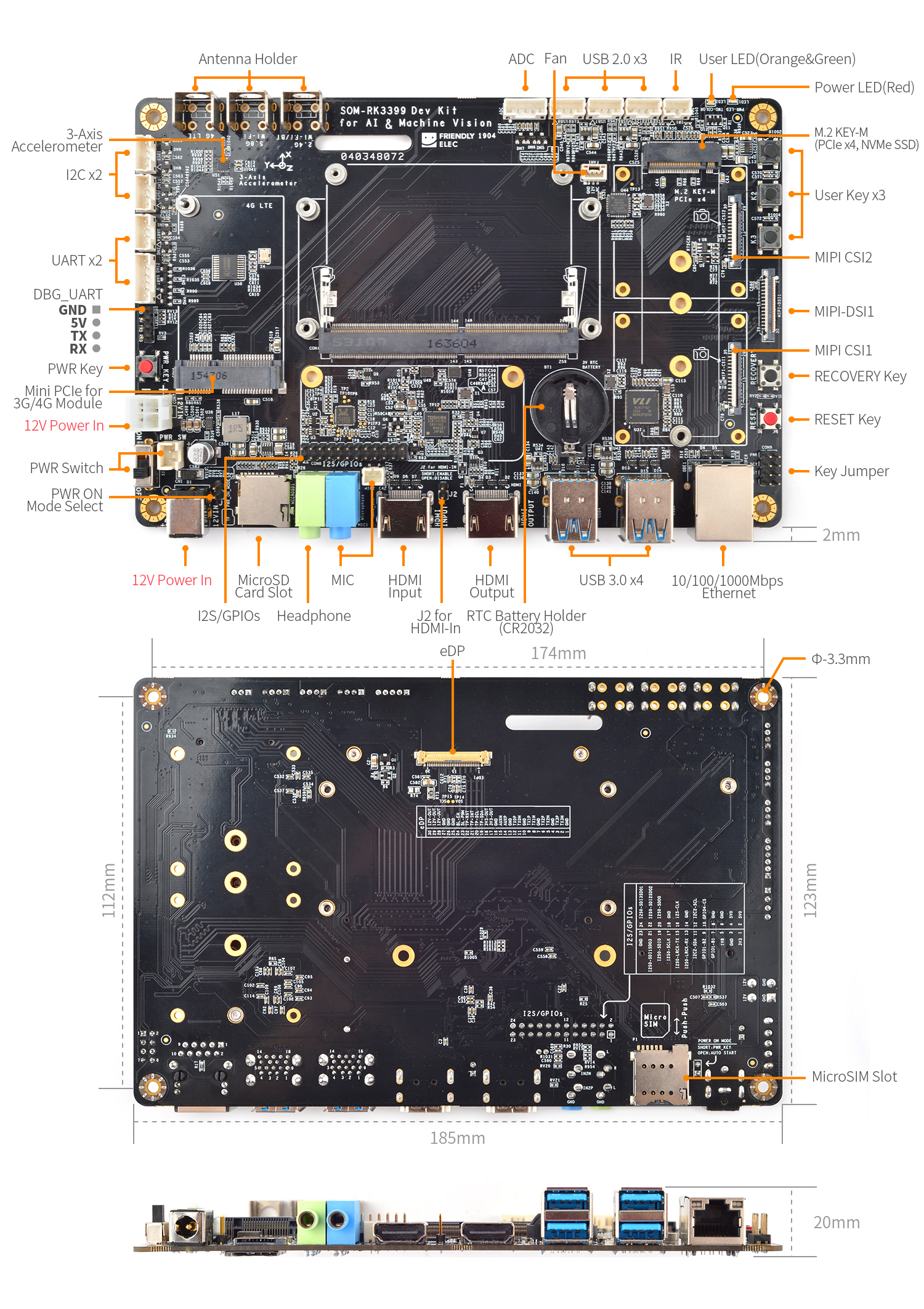
- The SOM-RK3399 module has various interfaces and ports. It can drive a 4-channel NVMe high speed SSD hard disk by working with a carrier board and the read/write rate can reach up to 1GB/s. It can drive dual-MIPI WDR cameras. It has an eDP interface, MIPI interface, USB 3.0, two USB 2.0 interfaces and other interfaces such as I2C, I2S, SPI, PWM, GPIO, serial and etc.
- The SOM-RK3399 can run popular OS systems such as Android 8.1, Ubuntu 18.04, Armbian and Buildroot smoothly. It has well established software support. Especially it has NN SDK packages for neural networks in Android 8.1, VPU hardware encoding/decoding in Qt-5.10, and GPU graphic acceleration. It supports development of dynamic GUI with Qt Quick. It is a perfect platform for startups to develop applications and prototypes in facial detection, machine vision, VR, autonomous-driving, deep learning, AI and etc.
2 Hardware Spec
- SoC: Rockchip RK3399
- CPU: big.LITTLE,Dual-Core Cortex-A72(up to 2.0GHz) + Quad-Core Cortex-A53(up to 1.5GHz)
- GPU: Mali-T864 GPU,supports OpenGL ES1.1/2.0/3.0/3.1, OpenVG1.1, OpenCL, DX11, and AFBC
- VPU: 4K VP9 and 4K 10bits H265/H264 60fps decoding, Dual VOP, etc
- PMU: RK808-D PMIC, cooperated with independent DC/DC, enabling DVFS, software power-down, RTC wake-up, system sleep mode
- RAM: Dual-Channel 2GB DDR3
- Flash: 16GB eMMC 5.1 Flash
- Ethernet: Native Gigabit Ethernet
- Wi-Fi/BT: 802.11a/b/g/n/ac, Bluetooth 4.1, Wi-Fi and Bluetooth combo module, dual antenna interface
- Video Input: one or two 4-Lane MIPI-CSI, dual ISP, up to 13MPix/s,supports simultaneous input of dual camera data
- Video output
- HDMI: HDMI 2.0a, supports 4K@60Hz,HDCP 1.4/2.2
- DP on Type-C: DisplayPort 1.2 Alt Mode on USB Type-C
- LCD Interface: one eDP 1.3(4-Lane,10.8Gbps), one or two 4-Lane MIPI-DSI
- USB
- USB 2.0: 2 independent native USB 2.0 Host
- USB 3.0: 1 native USB 3.0 Host
- USB Type-C: Supports USB3.0 Type-C and DisplayPort 1.2 Alt Mode on USB Type-C
- PCIe: PCIe x4, compatible with PCIe 2.1, Dual operation mode;
- SDIO/MMC: 1x SDIO/MMC for SD Card
- GPIOs, I2S, I2C, PWM, UART, SPI, ADCs
- 2 X 1.8V I2C, 1 x 3V I2C
- 1 x 3V UART/SPI
- 2 x PWM
- 1 x IR-RX
- 1 x SPDIF_TX
- 1 x 1.8V I2S,
- 6 x 1.8V GPIOs, 8 x 3V GPIOs
- ADC: 3 x 1.8V ADC inputs
- Debug: one Debug UART, 3V level, 1500000bps
- Keys: PowerKey, Reset, Recovery
- LED: 1 x power LED and 1 x GPIO Controlled LED
- Power supply: DC 12V/1A
- PCB: 8 Layer, 50 mm x 69.6 mm, 260 Pin edge connector
- Ambient Operating Temperature: -20℃ to 70℃
3 Software Features
4 Diagram, Layout and Dimension
- 260 Pin Spec
- Socket Type:0.5mm Pitch 260-Pin Standard Type DDR4 SODIMM Socket, refer to https://www.te.com/usa-en/product-2309409-5.html
| Top | Bottom | ||||||||
|---|---|---|---|---|---|---|---|---|---|
| Pin# | Assignment | Pin Type | If Not Use | Description | Pin# | Assignment | Pin Type | If Not Use | Description |
| 1 | VCC_IN | Power IN | / | 12V Power Input | 2 | VCC_IN | Power IN | / | 12V Power Input |
| 3 | VCC_IN | Power IN | / | 4 | VCC_IN | Power IN | / | ||
| 5 | VCC_IN | Power IN | / | 6 | VCC_IN | Power IN | / | ||
| 7 | VCC_IN | Power IN | / | 8 | VCC_IN | Power IN | / | ||
| 9 | GND | Power | / | System Ground(0V) | 10 | GND | Power | / | System Ground(0V) |
| 11 | GND | Power | / | 12 | GND | Power | / | ||
| 13 | VCC5V0_SYS | Power OUT | float | 5V Power Output,2A max. Auto on when system power on, and off when system power off. | 14 | PWR_KEY | In | float | System Power Key signal, active low, internal pulled up to 3.3V with 10K |
| 15 | VCC5V0_SYS | Power OUT | float | 16 | VDC_ONOFF | In | float | Power On Mode Select, float for Auto Start,short to GND for PowerKey Mode | |
| 17 | VCC5V0_SYS | Power OUT | float | 18 | RTC_BATT_IN | Power IN | float | RTC backup battery(3V)input,backup current is 25uA | |
| 19 | VCC5V0_SYS | Power OUT | float | 20 | RECOVERY | In | float | System RECOVERY Key signal,acticve low | |
| 21 | VCC3V3_SYS | Power OUT | float | 3.3V Power Output,1A max. Auto on when system power on, and off when system power off. | 22 | RESET_IN_H | In | float | RESET signal, acticve hight |
| 23 | VCC3V3_SYS | Power OUT | float | 24 | GND | Power | / | System Ground(0V) | |
| 25 | VCC3V3_SYS | Power OUT | float | 26 | ADC_IN0 | In | float | 0V to 1.8V inputs of RK3399 SoC ADC | |
| 27 | VCC3V3_SYS | Power OUT | float | 28 | ADC_IN2 | In | float | ||
| 29 | VCC_1V8 | Power OUT | float | 1.8V Power Output,200mA max. Auto on when system power on, and off when system power off. | 30 | ADC_IN3 | In | float | |
| 31 | VCC_1V8 | Power OUT | float | 32 | GND | Power | / | System Ground(0V) | |
| 33 | VCC3V3_S3 | Power OUT | float | 3.3V Power Output,100mA max. Auto on when system power on, and off when system sleep or power off. | 34 | GPIO1_A0 | In/Out | float | 3V GPIO. Linux GPIO 32 |
| 35 | GND | Power | / | System Ground(0V) | 36 | GPIO1_A1 | In/Out | float | 3V GPIO. Linux GPIO 33 |
| 37 | GPIO0_A2 | In/Out | float | 1.8V GPIO. Linux GPIO 2 | 38 | GPIO1_A3 | In/Out | float | 3V GPIO. Linux GPIO 35 |
| 39 | GPIO2_A2 | In/Out | float | 1.8V GPIO. Linux GPIO 2 | 40 | GPIO1_A4 | In/Out | float | 3V GPIO. Linux GPIO 36 |
| 41 | GPIO2_A3 | In/Out | float | 1.8V GPIO. Linux GPIO 67 | 42 | GPIO1_C2 | In/Out | float | 3V GPIO . Linux GPIO 50 |
| 43 | GPIO2_A4 | In/Out | float | 1.8V GPIO. Linux GPIO 68 | 44 | GPIO1_C6 | In/Out | float | 3V GPIO. Linux GPIO 54 |
| 45 | GPIO2_A5 | In/Out | float | 1.8V GPIO. Linux GPIO 69 | 46 | GPIO1_C7 | In/Out | float | 3V GPIO . Linux GPIO 55 |
| 47 | GPIO2_A6 | In/Out | float | 1.8V GPIO. Linux GPIO 70 | 48 | GPIO1_D0 | In/Out | float | 3V GPIO . Linux GPIO 56 |
| 49 | IR_RX | In | float | Infrared Receiver input, 1.8V level | 50 | GPIO4_C5/SPDIF_TX | In/Out | float | 3V GPIO . Linux GPIO 149. or SPDIF Output |
| 51 | GND | Power | / | System Ground(0V) | 52 | UART2DBG_TX | Out | float | Debug UART TX, 1500000bps, 3V level |
| 53 | I2C1_SCL | Out | float | I2C1 clock, 1.8V level, open drian with 2.2K pulled internal | 54 | UART2DBG_RX | In | float | Debug UART RX, 1500000bps, 3V level |
| 55 | I2C1_SDA | In/Out | float | I2C1 data, 1.8V level, open drian with 2.2K pulled internal | 56 | SPI1_CSn0 | Out | float | SPI1 chip select, 3V level |
| 57 | I2C2_SDA | In/Out | float | I2C2 data, 1.8V level, open drian with 2.2K pulled internal | 58 | SPI1_TXD/UART4_TX | Out | float | SPI1 MOSI, or UART4 TX,3V level |
| 59 | I2C2_SCL | Out | float | I2C2 clock, 1.8V level, open drian with 2.2K pulled internal | 60 | SPI1_RXD/UART4_RX | In | float | SPI1 MISO, or UART4 RX,3V level |
| 61 | I2C7_SCL_HDMI | Out | float | I2C7 clock, 1.8V level, for HDMI EDID CLK, open drian with 2.2K pulled internal | 62 | SPI1_CLK | Out | float | SPI1 Clock, 3V level |
| 63 | I2C7_SDA_HDMI | In/Out | float | I2C7 data, 1.8V level, for HDMI EDID DATA, open drian with 2.2K pulled internal | 64 | GND | Power | / | System Ground(0V) |
| 65 | GND | Power | / | System Ground(0V) | 66 | GPIO4_C1/I2C3_SCL | In/Out | float | I2C3 clock, 3V level,open drian. or GPIO,Linux GPIO 145 |
| 67 | I2S0_SCLK | Out | float | I2S0 continuous serial clock, 1.8V level | 68 | GPIO4_C0/I2C3_SDA | In/Out | float | I2C3 data, 3V level,open drian. or GPIO,Linux GPIO 144 |
| 69 | I2S0_LRCK_RX | Out | float | I2S0 word select for input data, 1.8V level | 70 | I2C4_TPSCL | Out | float | I2C4 clock,3V level, open drian with 2.2K pulled up,for touch panel |
| 71 | I2S0_LRCK_TX | Out | float | I2S0 word select for output data, 1.8V level | 72 | I2C4_TPSDA | In/Out | float | I2C4 data,3V level, open drian with 2.2K pulled up,for touch panel |
| 73 | I2S0_SDI0 | In | float | I2S0 serial data, 1.8V level | 74 | GND | Power | / | System Ground(0V) |
| 75 | I2S0_SDI1SDO3 | In/out | float | I2S0 serial data, 1.8V level | 76 | HP_DET_H | In | Pull up to VCC3V3_SYS | headphone insert detect, active hight |
| 77 | I2S0_SDI2SDO2 | In/out | float | I2S0 serial data, 1.8V level | 78 | GPIO4_D5_LCD_BL_EN | Out | float | LCD backlight on/off control, active hight, 3V level |
| 79 | I2S0_SDI3SDO1 | In/out | float | I2S0 serial data, 1.8V level | 80 | GPIO4_D6_LCD_RST_H | Out | float | LCD reset, active hight, 3V level. |
| 81 | I2S0_SDO0 | out | float | I2S0 serial data, 1.8V level | 82 | GPIO1_B5_TP_RST | Out | float | Touch panel reset, active low, 3V level |
| 83 | GND | Power | / | System Ground(0V) | 84 | GPIO1_C4_TP_INT | In | float | Touch panel IRQ, active low, 3V level |
| 85 | I2S_CLK | out | float | I2S Mclk for I2S0 and I2S1 | 86 | GND | Power | / | System Ground(0V) |
| 87 | GND | Power | / | System Ground(0V) | 88 | PWM0_BL | Out | float | PWM0 for LCD backlight dimming |
| 89 | I2S1_SCLK | Out | float | I2S1 continuous serial clock, 1.8V level | 90 | GPIO4_C6/PWM1 | Out | float | PWM1 for cooling fan control |
| 91 | 2S1_LRCK_RX | Out | float | I2S1 word select for input data, 1.8V level | 92 | GND | Power | / | System Ground(0V) |
| 93 | I2S1_LRCK_TX | Out | float | I2S1 word select for output data, 1.8V level | 94 | VCC3V0_SD | Power Out | float | 3V power out for SD card. |
| 95 | I2S1_SDI0 | In | float | I2S0 serial data, 1.8V level | 96 | GND | Power | / | System Ground(0V) |
| 97 | I2S1_SDO0 | Out | float | I2S0 serial data, 1.8V level | 98 | SDMMC0_D0 | In/Out | float | SD card Data0 |
| 99 | MIPI_CSI0_RST | Out | float | Camera Reset for MIPI CSI0, 1.8V level | 100 | SDMMC0_D1 | In/Out | float | SD card Data1 |
| 101 | MIPI_CSI0_PWN | Out | float | Camera Power Down for MIPI CSI0, 1.8V level | 102 | SDMMC0_D2 | In/Out | float | SD card Data2 |
| 103 | MIPI_CSI1_RST | Out | float | Camera Reset for MIPI CSI1, 1.8V level | 104 | SDMMC0_D3 | In/Out | float | SD card Data3 |
| 105 | MIPI_CSI1_PWN | Out | float | Camera Power Down for MIPI CSI1, 1.8V level | 106 | SDMMC0_CMD | Out | float | SD card CMD |
| 107 | VCC1V8_CAM | Power Out | float | Power Out for Camera IO | 108 | SDMMC0_DET_L | In | float | SD card detect |
| 109 | GND | Power | / | System Ground(0V) | 110 | GND | Power | / | System Ground(0V) |
| 111 | GPIO2_B3_CIF_CLKOUTA | Out | float | MCLK for camera sensor | 112 | SDMMC0_CLK | Out | float | SD card Clock |
| 113 | GND | Power | / | System Ground(0V) | 114 | GND | Power | / | System Ground(0V) |
| 115 | MIPI_RX0_D3N | In | float | MIPI CSI0 negative differential data line | 116 | MIPI_TX1/RX1_D0N | In/Out | float | MIPI CSI1/DSI1 negative differential data line |
| 117 | MIPI_RX0_D3P | In | float | MIPI CSI0
positive differential data line |
118 | MIPI_TX1/RX1_D0P | In/Out | float | MIPI CSI1/DSI1
positive differential data line |
| 119 | GND | Power | / | System Ground(0V) | 120 | GND | Power | / | System Ground(0V) |
| 121 | MIPI_RX0_D2N | In | float | MIPI CSI0 negative differential data line | 122 | MIPI_TX1/RX1_D1N | In/Out | float | MIPI CSI1/DSI1 negative differential data line |
| 123 | MIPI_RX0_D2P | In | float | MIPI CSI0
positive differential data line |
124 | MIPI_TX1/RX1_D1P | In/Out | float | MIPI CSI1/DSI1
positive differential data line |
| 125 | GND | Power | / | System Ground(0V) | 126 | GND | Power | / | System Ground(0V) |
| 127 | MIPI_RX0_CLKN | In | float | MIPI CSI0 negative differential clock line | 128 | MIPI_TX1/RX1_CLKN | In/Out | float | MIPI CSI1/DSI1 negative differential clock line |
| 129 | MIPI_RX0_CLKP | In | float | MIPI CSI0
positive differential clock line |
130 | MIPI_TX1/RX1_CLKP | In/Out | float | MIPI CSI1/DSI1
positive differential clock line |
| 131 | GND | Power | / | System Ground(0V) | 132 | GND | Power | / | System Ground(0V) |
| 133 | MIPI_RX0_D1N | In | float | MIPI CSI0 negative differential data line | 134 | MIPI_TX1/RX1_D2N | In/Out | float | MIPI CSI1/DSI1 negative differential data line |
| 135 | MIPI_RX0_D1P | In | float | MIPI CSI0
positive differential data line |
136 | MIPI_TX1/RX1_D2P | In/Out | float | MIPI CSI1/DSI1
positive differential data line |
| 137 | GND | Power | / | System Ground(0V) | 138 | GND | Power | / | System Ground(0V) |
| 139 | MIPI_RX0_D0N | In | float | MIPI CSI0 negative differential data line | 140 | MIPI_TX1/RX1_D3N | In/Out | float | MIPI CSI1/DSI1 negative differential data line |
| 141 | MIPI_RX0_D0P | In | float | MIPI CSI0
positive differential data line |
142 | MIPI_TX1/RX1_D3P | In/Out | float | MIPI CSI1/DSI1
positive differential data line |
| 143 | GND | Power | / | System Ground(0V) | 144 | GND | Power | / | System Ground(0V) |
| Connector Key | Connector Key | ||||||||
| 145 | HDMI_CEC | In/Out | float | HDMI CEC signal, 3V level | 146 | GND | Power | / | System Ground(0V) |
| 147 | HDMI_HPD | In | float | HDMI hot plug | 148 | MIPI_TX0_D3N | Out | float | MIPI DSI0 negetive differential data line |
| 149 | GND | Power | / | System Ground(0V) | 150 | MIPI_TX0_D3P | Out | float | MIPI DSI0 positive differential data line |
| 151 | HDMI_TXCN | Out | float | HDMI differential clock line negative | 152 | GND | Power | / | System Ground(0V) |
| 153 | HDMI_TXCP | Out | float | HDMI differential clock line positive | 154 | MIPI_TX0_D2N | Out | float | MIPI DSI0 negetive differential data line |
| 155 | GND | Power | / | System Ground(0V) | 156 | MIPI_TX0_D2P | Out | float | MIPI DSI0 positive differential data line |
| 157 | HDMI_TX0N | Out | float | HDMI differential data line negative | 158 | GND | Power | / | System Ground(0V) |
| 159 | HDMI_TX0P | Out | float | HDMI differential data line positive | 160 | MIPI_TX0_CLKN | Out | float | MIPI DSI0 negetive differential clock line |
| 161 | GND | Power | / | System Ground(0V) | 162 | MIPI_TX0_CLKP | Out | float | MIPI DSI0 positive differential clock line |
| 163 | HDMI_TX1N | Out | float | HDMI differential data line negative | 164 | GND | Power | / | System Ground(0V) |
| 165 | HDMI_TX1P | Out | float | HDMI differential data line positive | 166 | MIPI_TX0_D1N | Out | float | MIPI DSI0 negetive differential data line |
| 167 | GND | Power | / | System Ground(0V) | 168 | MIPI_TX0_D1P | Out | float | MIPI DSI0 positive differential data line |
| 169 | HDMI_TX2N | Out | float | HDMI differential data line negative | 170 | GND | Power | / | System Ground(0V) |
| 171 | HDMI_TX2P | Out | float | HDMI differential data line positive | 172 | MIPI_TX0_D0N | Out | float | MIPI DSI0 negetive differential data line |
| 173 | GND | Power | / | System Ground(0V) | 174 | MIPI_TX0_D0P | Out | float | MIPI DSI0 positive differential data line |
| 175 | USB3.0/TYPE-C1_DP | In/Out | float | TYPEC1 USB 2.0 data+ | 176 | GND | Power | / | System Ground(0V) |
| 177 | USB3.0/TYPE-C1_DM | In/Out | float | TYPEC1 USB 2.0 data- | 178 | PCIE_RX3_N | In | float | PCIe negative differential data line |
| 179 | GND | Power | / | System Ground(0V) | 180 | PCIE_RX3_P | In | float | PCIe positive differential data line |
| 181 | USB3.0/TYPEC1_TX1P | Out | float | TYPEC1 USB3.0 PHY0 SuperSpeed TX1P | 182 | GND | Power | / | System Ground(0V) |
| 183 | USB3.0/TYPEC1_TX1M | Out | float | TYPEC1 USB3.0 PHY0 SuperSpeed TX1M | 184 | PCIE_TX3N | Out | float | PCIe negative differential data line |
| 185 | GND | Power | / | System Ground(0V) | 186 | PCIE_TX3P | Out | float | PCIe positive differential data line |
| 187 | USB3.0/TYPEC1_RX1P | In | float | TYPEC1 USB3.0 PHY0 SuperSpeed RX1P | 188 | GND | Power | / | System Ground(0V) |
| 189 | USB3.0/TYPEC1_RX1M | In | float | TYPEC1 USB3.0 PHY0 SuperSpeed RX1M | 190 | PCIE_RX2_N | In | float | PCIe negative differential data line |
| 191 | GND | Power | / | System Ground(0V) | 192 | PCIE_RX2_P | In | float | PCIe positive differential data line |
| 193 | TYPEC1_TX2P | Out | float | TYPEC1 USB3.0 PHY0 SuperSpeed TX2P | 194 | GND | Power | / | System Ground(0V) |
| 195 | TYPEC1_TX2M | Out | float | TYPEC1 USB3.0 PHY0 SuperSpeed TX2M | 196 | PCIE_TX2N | Out | float | PCIe negative differential data line |
| 197 | GND | Power | / | System Ground(0V) | 198 | PCIE_TX2P | Out | float | PCIe positive differential data line |
| 199 | TYPEC1_RX2P | In | float | TYPEC1 USB3.0 PHY0 SuperSpeed RX2P | 200 | GND | Power | / | System Ground(0V) |
| 201 | TYPEC1_RX2M | In | float | TYPEC1 USB3.0 PHY0 SuperSpeed RX2M | 202 | PCIE_RX1_N | In | float | PCIe negative differential data line |
| 203 | GND | Power | / | System Ground(0V) | 204 | PCIE_RX1_P | In | float | PCIe positive differential data line |
| 205 | TYPEC1_SBU1 | In/Out | float | TYPEC1 SBU1 | 206 | GND | Power | / | System Ground(0V) |
| 207 | TYPEC1_SBU2 | In/Out | float | TYPEC1 SBU2 | 208 | PCIE_TX1N | Out | float | PCIe negative differential data line |
| 209 | GND | Power | / | System Ground(0V) | 210 | PCIE_TX1P | Out | float | PCIe positive differential data line |
| 211 | TYPEC1_SBU1_DC | Out | float | TYPEC1 SBU1 DC Bias | 212 | GND | Power | / | System Ground(0V) |
| 213 | TYPEC1_SBU2_DC | Out | float | TYPEC1 SBU2 DC Bias | 214 | PCIE_RX0_N | In | float | PCIe negative differential data line |
| 215 | TYPEC1_U2VBUSDET | In | float | TYPEC1 Vbus detect | 216 | PCIE_RX0_P | In | float | PCIe positive differential data line |
| 217 | GND | Power | / | System Ground(0V) | 218 | GND | Power | / | System Ground(0V) |
| 219 | HOST0_DP | In/Out | float | USB 2.0 Host0 data+ | 220 | PCIE_TX0N | Out | float | PCIe negative differential data line |
| 221 | HOST0_DM | In/Out | float | USB 2.0 Host0 data- | 222 | PCIE_TX0P | Out | float | PCIe positive differential data line |
| 223 | GND | Power | / | System Ground(0V) | 224 | GND | Power | / | System Ground(0V) |
| 225 | HOST1_DP | In/Out | float | USB 2.0 Host1 data+ | 226 | PCIE_REF_CLKN | Out | float | PCIe negative differential reference clock line |
| 227 | HOST1_DM | In/Out | float | USB 2.0 Host1 data- | 228 | PCIE_REF_CLKP | Out | float | PCIe positive differential reference clock line |
| 229 | GND | Power | / | System Ground(0V) | 230 | GND | Power | / | System Ground(0V) |
| 231 | EDP_TX3N | Out | float | eDP data line negative | 232 | LAN_LED0_BLINK | Out | float | 10/100/1000M Ethernet Status LED0 |
| 233 | EDP_TX3P | Out | float | eDP data line positive | 234 | LAN_LED1_LINK | Out | float | 10/100/1000M Ethernet Status LED1 |
| 235 | GND | Power | / | System Ground(0V) | 236 | GND | Power | / | System Ground(0V) |
| 237 | EDP_TX2N | Out | float | eDP data line negative | 238 | MDI3- | In/Out | float | 10/100/1000M Ethernet MDI3- |
| 239 | EDP_TX2P | Out | float | eDP data line positive | 240 | MDI3+ | In/Out | float | 10/100/1000M Ethernet MDI3+ |
| 241 | GND | Power | / | System Ground(0V) | 242 | GND | Power | / | System Ground(0V) |
| 243 | EDP_TX1N | Out | float | eDP data line negative | 244 | MDI2- | In/Out | float | 10/100/1000M Ethernet MDI2- |
| 245 | EDP_TX1P | Out | float | eDP data line positive | 246 | MDI2+ | In/Out | float | 10/100/1000M Ethernet MDI2+ |
| 247 | GND | Power | / | System Ground(0V) | 248 | GND | Power | / | System Ground(0V) |
| 249 | EDP_TX0N | Out | float | eDP data line negative | 250 | MDI1- | In/Out | float | 10/100/1000M Ethernet MDI1- |
| 251 | EDP_TX0P | Out | float | eDP data line positive | 252 | MDI1+ | In/Out | float | 10/100/1000M Ethernet MDI1+ |
| 253 | GND | Power | / | System Ground(0V) | 254 | GND | Power | / | System Ground(0V) |
| 255 | EDP_AUXP | In/Out | float | eDP AUX line positive | 256 | MDI0- | In/Out | float | 10/100/1000M Ethernet MDI0- |
| 257 | EDP_AUXN | In/Out | float | eDP AUX line negative | 258 | MDI0+ | In/Out | float | 10/100/1000M Ethernet MDI0+ |
| 259 | GND | Power | / | System Ground(0V) | 260 | GND | Power | / | System Ground(0V) |
5 Carrier Board
6 Link to Rockchip Resources
- Link to Rockchip's resources: https://gitlab.com/friendlyelec/rk3399-nougat/tree/nanopc-t4-nougat/RKDocs
- RK3399 datasheet V1.6
- RK3399TRM V1.4
7 Schematic, PCB CAD File
- Schematic: SOM-RK3399_1904_Schematic.pdf
- PCB CAD File:SOM-RK3399_1904_dxf.zip
