Difference between revisions of "NanoPi A64"
From FriendlyELEC WiKi
(→Introduction) |
(→Introduction) |
||
| Line 2: | Line 2: | ||
==Introduction== | ==Introduction== | ||
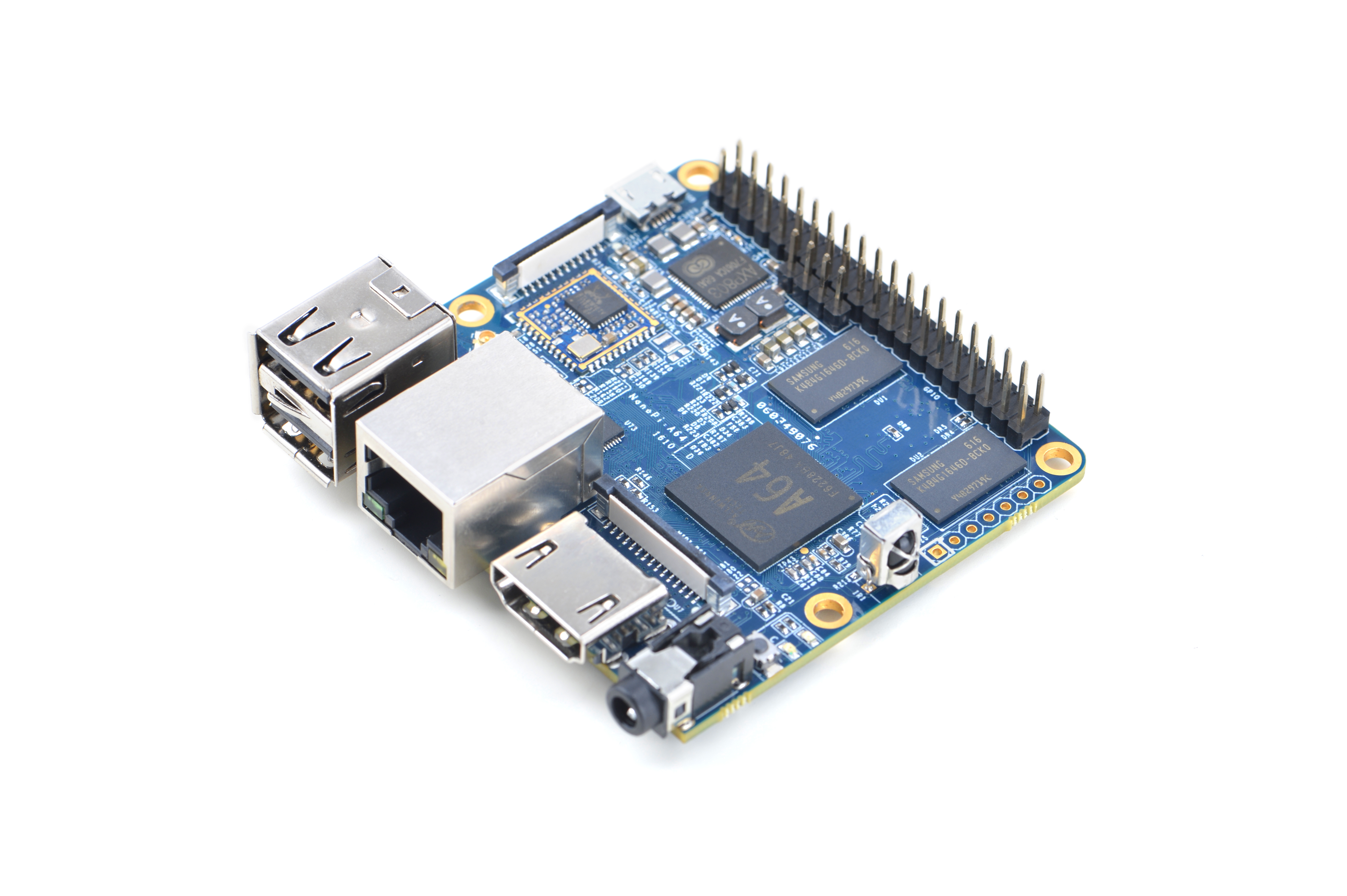
| − | [[File:NanoPi A64-1.jpg|thumb|frameless|300px| | + | [[File:NanoPi A64-1.jpg|thumb|frameless|300px|Overview]] |
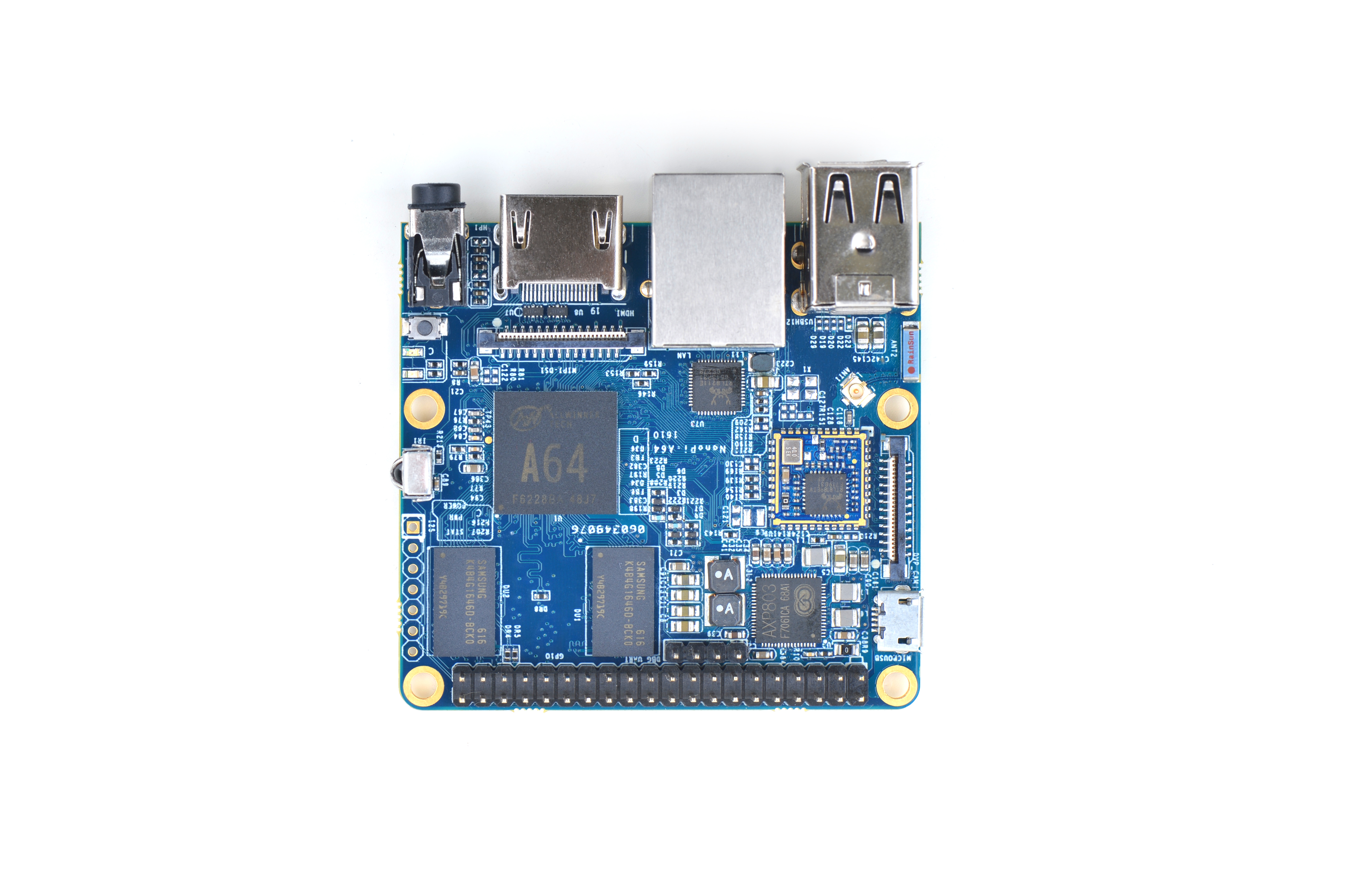
| − | [[File:NanoPi A64-2.jpg|thumb|frameless|300px| | + | [[File:NanoPi A64-2.jpg|thumb|frameless|300px|Obverse]] |
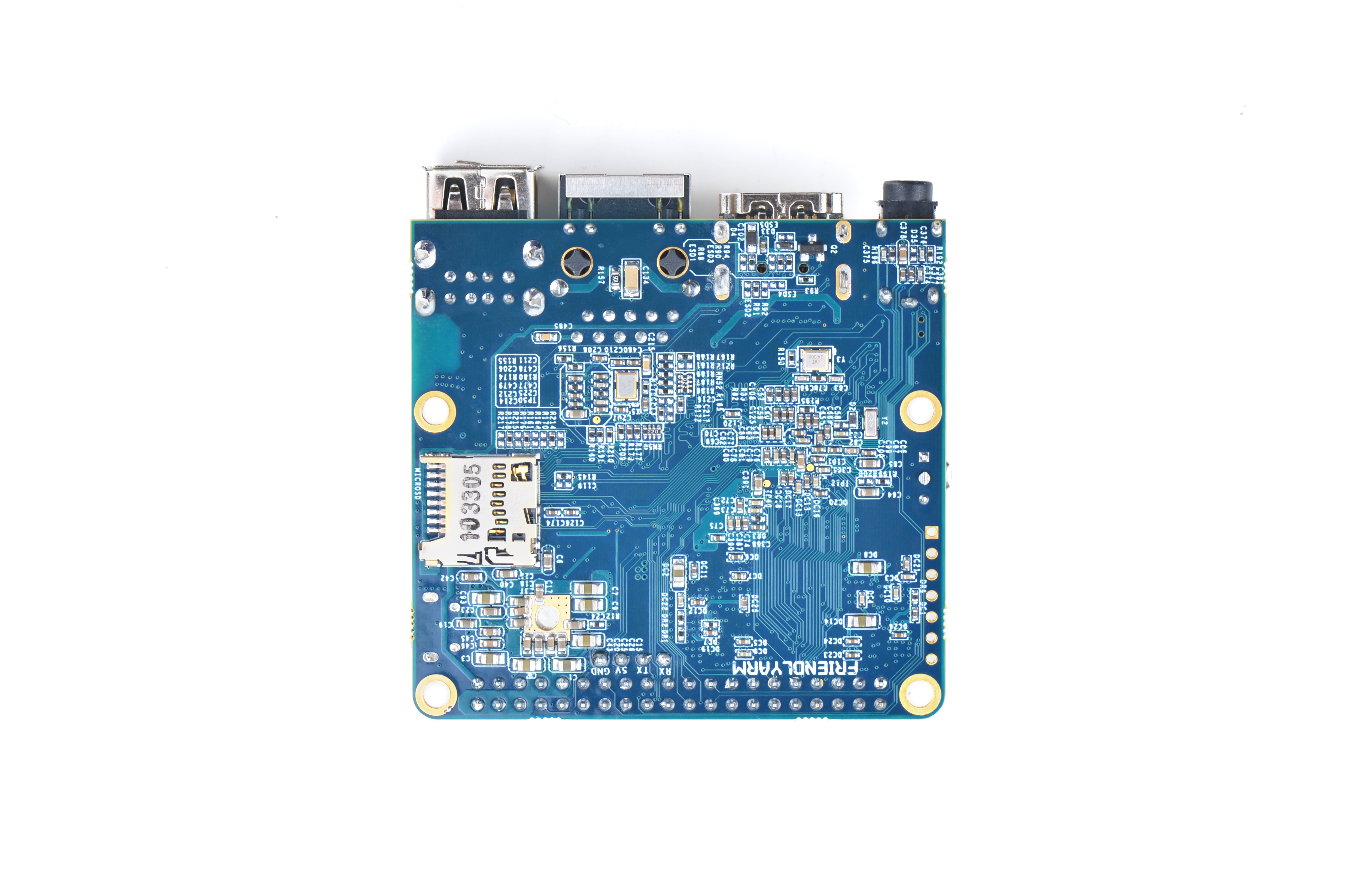
| − | [[File:NanoPi A64-3.jpg|thumb|frameless|300px| | + | [[File:NanoPi A64-3.jpg|thumb|frameless|300px|Reverse]] |
[[File:NanoPi A64-4.jpg|thumb|frameless|300px|外壳]] | [[File:NanoPi A64-4.jpg|thumb|frameless|300px|外壳]] | ||
The NanoPi A64 is a new board of high performance with low cost designed by FriendlyElec. It uses Allwinner’s A64 quad-core SoC(ARM Cortex-A53). FriendlyElec has made a UbuntuCore and a UbuntuMATE image files for it. | The NanoPi A64 is a new board of high performance with low cost designed by FriendlyElec. It uses Allwinner’s A64 quad-core SoC(ARM Cortex-A53). FriendlyElec has made a UbuntuCore and a UbuntuMATE image files for it. | ||
Revision as of 15:25, 23 December 2016
Contents
1 Introduction
The NanoPi A64 is a new board of high performance with low cost designed by FriendlyElec. It uses Allwinner’s A64 quad-core SoC(ARM Cortex-A53). FriendlyElec has made a UbuntuCore and a UbuntuMATE image files for it.
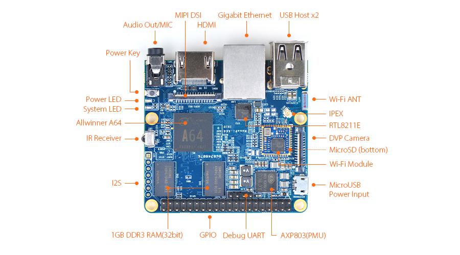
The NanoPi A64 is a small board with comprehensive interfaces, ports and features. It has Ethernet, IR receiver, Video/Audio input and output. It has onboard AXP803 PMU and WiFi. It takes power input from its MicroUSB port. It has MIPI-DSI and DVP interfaces, GPIO pin-header compatible with Raspberry Pi and a serial debug port.
2 Hardware Spec
- CPU: Allwinner A64, Quad-core Cortex-A53@648MHz to 1.152GHz, DVFS
- GPU: Mali400MP2, Supports OpenGL ES2.0, OpenVG1.1
- DDR3 RAM: 1GB
- Ethernet: One Gigabit Ethernet (RTL8211E)
- PMU Power Management: AXP803, support software power-off
- Wi-Fi: 802.11b/g/n
- Audio Out/MIC: 3.5mm audio jack
- IR Receiver: Onboard IR receiver
- USB 2.0 Type A x 2
- Serial Debug Port: 2.54mm pitch 4pin-header
- microSD Slot x 1
- microUSB x 1: only for power input
- DVP Camera: 0.5mm pitch 24pin FPC seat
- Video Out: 1.4 HDMI Type-A
- MIPI DSI: 0.5mm pitch 30pin FPC seat
- GPIO: 2.54mm pitch 40pin-header, compatible with Raspberry Pi's GPIO. It includes UART, SPI, I2C, PWM, IO etc
- I2S: 7pin, 2.54mm pitch
- Power Button x 1
- LED: Power Indication x 1, System LED x 1
- PCB : Six layer, ENIG
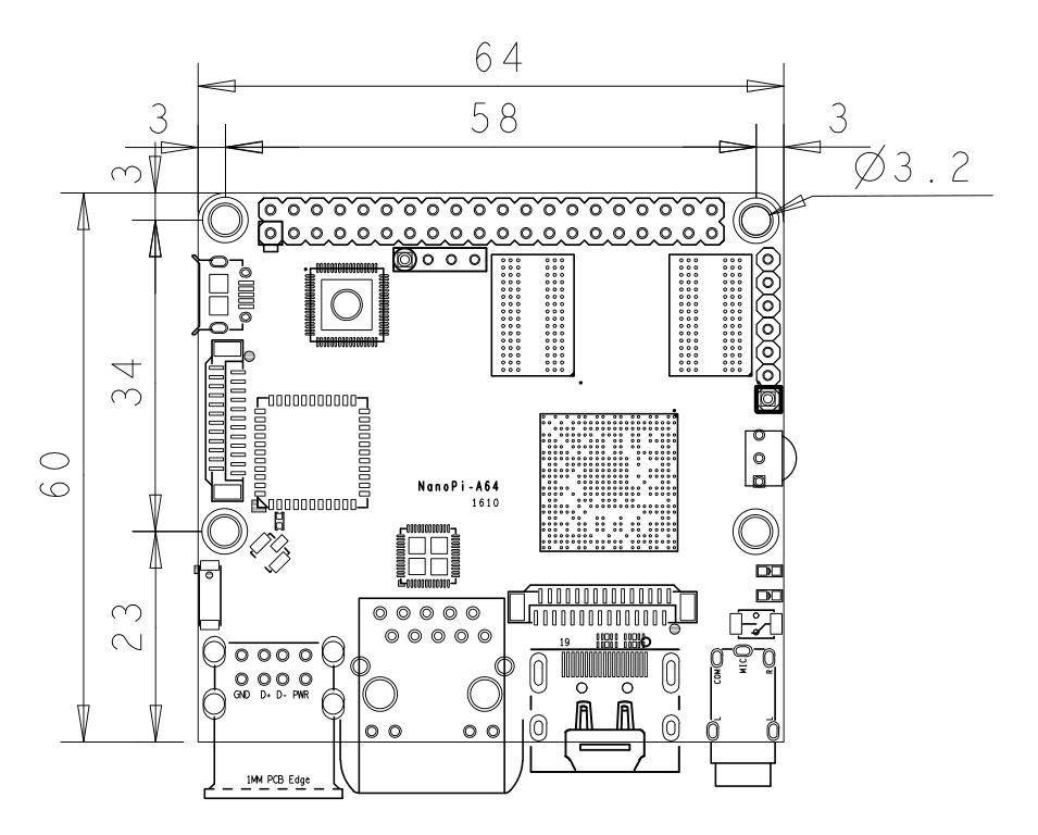
- Dimension: 64 x 60mm
- Power: DC 5V/2A
- OS: Ubuntu-Core with QtE, Ubuntu-MATE
3 Diagram, Layout and Dimension
3.1 Layout
- GPIO Pin Description
Pin# Name Pin# Name 1 SYS_3.3V 2 VDD_5V 3 GPIOE15/I2C2_SDA 4 VDD_5V 5 GPIOE14/I2C2_SCL 6 GND 7 GPIOD7 8 GPIOH4/UART3-TX 9 GND 10 GPIOH5/UART3-RX 11 GPIOB0/UART2-TX 12 GPIOL10/PWM_S 13 GPIOL8/I2C_S_SCL 14 GND 15 GPIOL9/I2C_S_SDA 16 GPIOH6/UART3-RTS 17 SYS_3.3V 18 GPIOH7/UART3-CTS 19 GPIOC0/SPI0-MOSI 20 GND 21 GPIOC1/SPI0-MISO 22 GPIOB1/UART2-RX 23 GPIOC2/SPI0-CLK 24 GPIOC3/SPI0-CS 25 GND 26 GPIOH8/SPDIF-OUT 27 GPIOH3/I2C1_SDA 28 GPIOH2/I2C1_SCL 29 GOIOH10 30 GND 31 GOIOH11 32 GPIOD4 33 GPIOD5 34 GND 35 GPIOD3/SPI1-MISO 36 GPIOD0/SPI1-CS 37 GPIOD6 38 GPIOD2/SPI1-MOSI 39 GND 40 GPIOD1/SPI1-CLK
- Debug Port(UART0)
Pin# Name 1 GND 2 VDD_5V 3 UART0-TX 4 UART0-RX
- I2S/PCM Pin Description
Pin# Name 1 GND 2 SYS_3.3V 3 GPIOB5/PCM0-BCLK 4 GPIOB4/PCM0-SYNC 5 GPIOB6/PCM0-DOUT 6 GPIOB7/PCM0-DIN 7 GPIOB3/I2S0-MCLK
- DVP Camera IF Pin Description
Pin# Name Description 1, 2 SYS_3.3V 3.3V power output 7,9,13,15,24 GND Ground, 0V 3 CAM_SCL I2C Clock 4 CAM_SDA I2C Data 5 GPIOE17 Regular GPIO, control signals output to camera modules 6 GPIOE16 Regular GPIO, control signals output to camera modules 8 MCLK Clock signals output to camera modules 10 NC Not Connected 11 VSYNC Vertical synchronization to CPU from camera modules 12 HREF/HSYNC HREF/HSYNC signal to CPU from camera modules 14 PCLK PCLK signal to CPU from camera modules 16-23 Data bit7-0 data signals
- MIPI-DSI Pin Description
Pin# Name Description 1, 2, 3 VDD_5V 5V power output 4,7,9,11,14,15,18,21,24,27,30 GND Ground, 0V 5 I2C0_SDA I2C Clock 6 I2C0_SCL I2C Data 8 GPIOL7 Regular GPIO 10 GPIOB2 Regular GPIO 12 GPIOL12 Regular GPIO 13 AP-RESET# System Reset 16 MIPI-DSI-D3N MIPI DSI数据, 差分信号负 17 MIPI-DSI-D3P MIPI DSI数据, 差分信号正 19 MIPI-DSI-D2N MIPI DSI数据, 差分信号负 20 MIPI-DSI-D2P MIPI DSI数据, 差分信号正 22 MIPI-DSI-D1N MIPI DSI数据, 差分信号负 23 MIPI-DSI-D1P MIPI DSI数据, 差分信号正 25 MIPI-DSI-D0N MIPI DSI数据, 差分信号负 26 MIPI-DSI-D0P MIPI DSI数据, 差分信号正 28 MIPI-DSI-CKN MIPI DSI时钟, 差分信号负 29 MIPI-DSI-CKP MIPI DSI时钟, 差分信号正
- Note
- SYS_3.3V: 3.3V power output. In our test the real output was 3.1V
- VDD_5V: 5V power input/output. The input range is 4.7V ~ 5.6V. It can take power input from the MicroUSB or the VDD_5V pin from the Debug Port. The VDD_5V is connected to MicroUSB's VBUS
- All pins are 3.3V(In our test the real output was 3.1V), output current is 5mA
- For more details refer to the document schematics
3.2 Dimensional Diagram
- 详细尺寸:dxf文件
