Difference between revisions of "NanoPi NEO4"
From FriendlyELEC WiKi
(Created page with "查看中文") |
|||
| Line 1: | Line 1: | ||
[[NanoPi NEO4/zh|查看中文]] | [[NanoPi NEO4/zh|查看中文]] | ||
| + | ==Introduction== | ||
| + | [[File:NanoPi NEO4-01B.jpg|thumb|Overview]] | ||
| + | [[File:NanoPi NEO4-A01.jpg|thumb|Front]] | ||
| + | [[File:NanoPi NEO4-B01.jpg|thumb|Back]] | ||
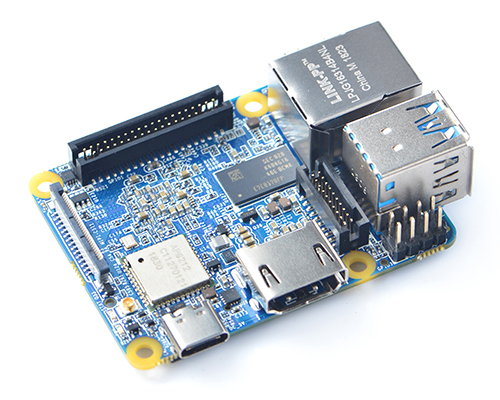
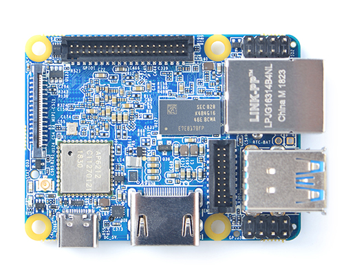
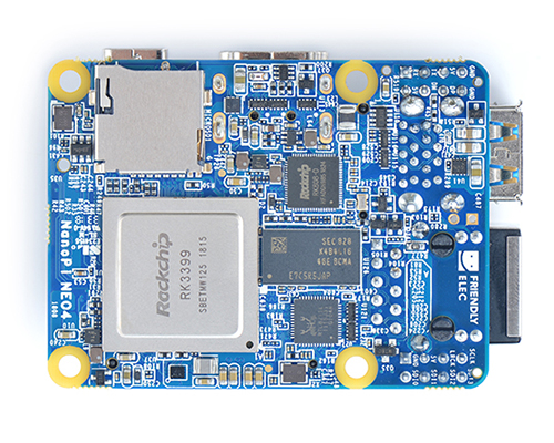
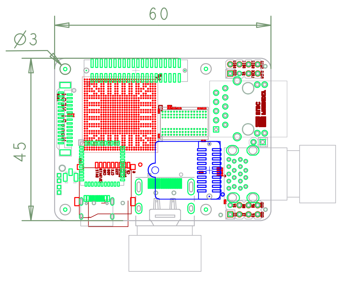
| + | *The NanoPi NEO4 is a RK3399 SoC based ARM board. Its PCB size is only 60 x 45 mm and has rich hardware resources. These features make it a good platform for rapid product prototyping and various applications. | ||
| + | *NanoPi NEO4 has 1GB RAM, an onboard 2.4G wireless module, and rich hardware resources, such as USB3.0, USB2.0, PCIe, GbE, HDMI, MIPI-CSI, eMMC socket, SPI, GPIO, I2C, PWM, RTC, UART, etc. | ||
| + | *NanoPi NEO4 can be booted from either a TF card or an external eMMC module. | ||
| + | *The NanoPi NEO4 supports Ubuntu Desktop 18.04(64-bit), Lubuntu 16.04(32-bit), Ubuntu Core 18.04(64-bit) and Lubuntu Desktop with GPU and VPU acceleration. With these rich resources and powerful performance it can be widely used in applications of machine learning, AI, deep learning, robots, industrial control, industrial cameras, advertisement machines, game machines, blockchain and etc. | ||
| + | |||
| + | ==Hardware Spec== | ||
| + | * SoC: Rockchip RK3399 | ||
| + | ** CPU: big.LITTLE,Dual-Core Cortex-A72(up to 2.0GHz) + Quad-Core Cortex-A53(up to 1.5GHz) | ||
| + | ** GPU: Mali-T864 GPU,supports OpenGL ES1.1/2.0/3.0/3.1, OpenVG1.1, OpenCL, DX11, and AFBC | ||
| + | ** VPU: 4K VP9 and 4K 10bits H265/H264 60fps decoding, Dual VOP, etc | ||
| + | * PMU: RK808-D PMIC, cooperated with independent DC/DC, enabling DVFS, solfware power-down, RTC wake-up, system sleep mode | ||
| + | * RAM: 1GB DDR3-1866 | ||
| + | * Flash: no Onboard eMMC, but has a eMMC socket | ||
| + | * Ethernet: Native Gigabit Ethernet | ||
| + | * Wi-Fi/BT: 802.11a/b/g/n, Bluetooth 4.0 combo module | ||
| + | * Video Input: one 4-Lane MIPI-CSI, up to 13MP | ||
| + | * Video output: HDMI: HDMI 2.0a, supports 4K@60Hz,HDCP 1.4/2.2 | ||
| + | * Audio Out: HDMI | ||
| + | * USB 3.0: 1x USB 3.0 Host Type-A | ||
| + | * USB 2.0: 2x USB 2.0 Host, one is Type-A, the other is 2.54mm header | ||
| + | * USB Type-C: Supports USB2.0 OTG and Power input | ||
| + | * microSD Slot x 1 | ||
| + | * GPIO1, 40Pin GPIO: | ||
| + | ** 2 X 3V I2C, 1x 3V UART/SPI, 1 x SPDIF_TX, up to 8 x 3V GPIOs | ||
| + | ** PCIe x2 | ||
| + | ** PWM x1, PowerKey | ||
| + | * GPIO2: | ||
| + | ** 1 x 1.8V 8ch-I2S | ||
| + | * GPIO3: | ||
| + | ** debug uart, 3V level, 1500000bps | ||
| + | ** USB 2.0 x1 | ||
| + | * LED: 1 x power LED and 1 x GPIO Controled LED | ||
| + | * RTC Battery: 2 Pin 1.27/1.25mm RTC battery input connector | ||
| + | * Power supply: 5V/3A | ||
| + | * PCB: 8 Layer, 60 mm x 45 mm | ||
| + | * Ambient Operating Temperature: -20℃ to 70℃ | ||
| + | |||
| + | ==Diagram, Layout and Dimension== | ||
| + | ===Layout=== | ||
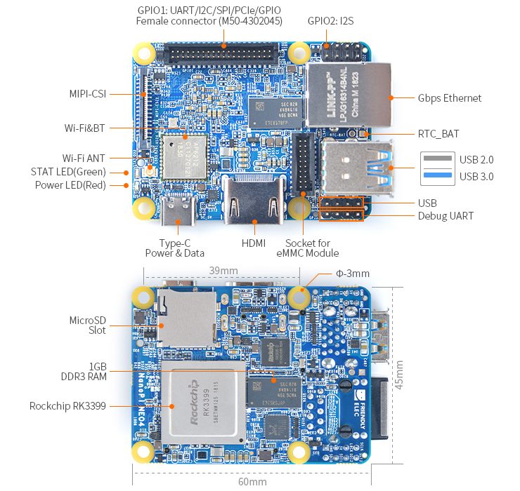
| + | [[File:NanoPi NEO4-1808-IF-01.jpg |thumb|600px|NanoPi NEO4 Layout]] | ||
| + | * '''GPIO1,40-Pin Spec''' | ||
| + | ::{| class="wikitable" | ||
| + | |- | ||
| + | |'''Pin#''' || '''Assignment''' ||'''Pin#''' || '''Assignment''' | ||
| + | |- | ||
| + | |1 || VCC3V3_SYS ||2 || VDD_5V | ||
| + | |- | ||
| + | |3 || I2C2_SDA(3V) ||4 || VDD_5V | ||
| + | |- | ||
| + | |5 || I2C2_SCL(3V) ||6 || GND | ||
| + | |- | ||
| + | |7 || GPIO1_A0(3V) ||8 || GPIO4_C1/I2C3_SCL(3V) | ||
| + | |- | ||
| + | |9 || GND ||10 || GPIO4_C0/I2C3_SDA(3V) | ||
| + | |- | ||
| + | |11 || GPIO1_A1(3V) ||12 || GPIO1_C2(3V) | ||
| + | |- | ||
| + | |13 || GPIO1_A3(3V) ||14 || GND | ||
| + | |- | ||
| + | |15 || GPIO1_A4(3V) ||16 || GPIO1_C6(3V) | ||
| + | |- | ||
| + | |17 || VCC3V3_SYS ||18 || GPIO1_C7(3V) | ||
| + | |- | ||
| + | |19 || SPI1_TXD/UARNEO4_TX(3V) ||20 || GND | ||
| + | |- | ||
| + | |21 || SPI1_RXD/UARNEO4_RX(3V) ||22 || GPIO1_D0(3V) | ||
| + | |- | ||
| + | |23 || SPI1_CLK(3V) ||24 || SPI1_CSn0(3V) | ||
| + | |- | ||
| + | |25 || GND ||26 || GPIO4_C5/SPDIF_TX(3V) | ||
| + | |- | ||
| + | |27 || PCIE_REF_CLKP ||28 || GPIO4_C6/PWM1(3V) | ||
| + | |- | ||
| + | |29 || PCIE_REF_CLKN ||30 || PWR_KEY | ||
| + | |- | ||
| + | |31 || GND ||32 || GND | ||
| + | |- | ||
| + | |33 || PCIE_TX0P ||34 || PCIE_TX1P | ||
| + | |- | ||
| + | |35 || PCIE_TX0N ||36 || PCIE_TX1N | ||
| + | |- | ||
| + | |37 || PCIE_RX0_P ||38 || PCIE_RX1_P | ||
| + | |- | ||
| + | |39 || PCIE_RX0_N ||40 || PCIE_RX1_N | ||
| + | |} | ||
| + | |||
| + | * '''GPIO2,8-Pin I2S Spec''' | ||
| + | :: I2S signals is 1.8V level | ||
| + | ::{| class="wikitable" | ||
| + | |- | ||
| + | |'''Pin#''' ||'''Assignment''' ||'''Pin#''' ||'''Assignment''' | ||
| + | |- | ||
| + | |1 || GND || 2 || I2S0_SDI0 | ||
| + | |- | ||
| + | |3 || VCC5V0_SYS || 4 || I2S0_SDI1SDO3 | ||
| + | |- | ||
| + | |5 || I2S0_LRCK_RX || 6 || I2S0_SDI2SDO2 | ||
| + | |- | ||
| + | |7 || I2S0_SCLK || 8 || I2S0_SDI3SDO1 | ||
| + | |} | ||
| + | |||
| + | * '''GPIO3,8-Pin UART/USB Spec''' | ||
| + | :: debug uart is 3V level, 1500000bps | ||
| + | ::{| class="wikitable" | ||
| + | |- | ||
| + | |'''Pin#''' ||'''Assignment''' || '''Description ''' ||'''Pin#''' ||'''Assignment''' || '''Description ''' | ||
| + | |- | ||
| + | |1 || UART2DBG_RX || debug uart intput || 2 || VCC5V0_SYS || 5V power output | ||
| + | |- | ||
| + | |3 || UART2DBG_TX || debug uart output || 4 || HOST1_DM || USB 2.0 data - | ||
| + | |- | ||
| + | |5 || VCC5V0_SYS || 5V power output || 6 || HOST1_DP || USB 2.0 data + | ||
| + | |- | ||
| + | |7 || GND || 0V || 8 || GND || 0V | ||
| + | |} | ||
| + | |||
| + | * '''MIPI-CSI Interface Pin Spec''' | ||
| + | :: 0.5mm FPC Connector | ||
| + | ::{| class="wikitable" | ||
| + | |- | ||
| + | |'''Pin#''' || '''MIPI-CSI1''' || '''Description ''' | ||
| + | |- | ||
| + | |1 || VCC5V0_SYS || 5V Power ouput | ||
| + | |- | ||
| + | |2 || VCC5V0_SYS || 5V Power ouput | ||
| + | |- | ||
| + | |3 || GND || Return current path | ||
| + | |- | ||
| + | |4 || VCC_CSI_AF2.8V || 2.8V Power for VCM | ||
| + | |- | ||
| + | |5 || VCC_CSI_1.2V || 1.2V Power for image sensor core circuit | ||
| + | |- | ||
| + | |6 || VCC1V8_CAM || 1.8V power for I/O circuit | ||
| + | |- | ||
| + | |7 || VCC_CSI_2.8V || 2.8V power for image sensor analog circuit | ||
| + | |- | ||
| + | |8 || VCC_CSI_1.0V || 1.0V Power for image sensor core circuit | ||
| + | |- | ||
| + | |9 || I2C1_SCL || 1.8V I2C clock signal | ||
| + | |- | ||
| + | |10 || I2C1_SDA || 1.8V I2C data signal | ||
| + | |- | ||
| + | |11 || MIPI_CSI0_RST || reset camera module | ||
| + | |- | ||
| + | |12 || MIPI_CSI0_PWN || Power down camera module | ||
| + | |- | ||
| + | |13 || GND || Return current path | ||
| + | |- | ||
| + | |14 || GPIO2_B3_CIF_CLKOUTA || MCLK to camera module | ||
| + | |- | ||
| + | |15 || GND || Return current path | ||
| + | |- | ||
| + | |16 || MIPI_RX0_D3P || MIPI CSI positive differential data line transceiver output | ||
| + | |- | ||
| + | |17 || MIPI_RX0_D3N || MIPI CSI negative differential data line transceiver output | ||
| + | |- | ||
| + | |18 || GND || Return current path | ||
| + | |- | ||
| + | |19 || MIPI_RX0_D2P ||MIPI CSI positive differential data line transceiver output | ||
| + | |- | ||
| + | |20 || MIPI_RX0_D2N || MIPI CSI negative differential data line transceiver output | ||
| + | |- | ||
| + | |21 || GND || Return current path | ||
| + | |- | ||
| + | |22 || MIPI_RX0_D1P || MIPI CSI positive differential data line transceiver output | ||
| + | |- | ||
| + | |23 || MIPI_RX0_D1N || MIPI CSI negative differential data line transceiver output | ||
| + | |- | ||
| + | |24 || GND || Return current path | ||
| + | |- | ||
| + | |25 || MIPI_RX0_CLKP || MIPI CSI positive differential clock line transceiver output | ||
| + | |- | ||
| + | |26 || MIPI_RX0_CLKN || MIPI CSI negative differential clock line transceiver output | ||
| + | |- | ||
| + | |27 || GND || Return current path | ||
| + | |- | ||
| + | |28 || MIPI_RX0_D0P ||MIPI CSI positive differential data line transceiver output | ||
| + | |- | ||
| + | |29 || MIPI_RX0_D0N || MIPI CSI negative differential data line transceiver output | ||
| + | |- | ||
| + | |30 || GND || Return current path | ||
| + | |} | ||
| + | |||
| + | * '''eMMC Socket Pin Spec''' | ||
| + | ::{| class="wikitable" | ||
| + | |- | ||
| + | |'''Pin#''' || '''Assignment''' ||'''Pin#''' || '''Assignment''' | ||
| + | |- | ||
| + | |1 || EMMC_D0 ||2 || EMMC_D1 | ||
| + | |- | ||
| + | |3 || EMMC_D2 ||4 || EMMC_D3 | ||
| + | |- | ||
| + | |5 || EMMC_D4 ||6 || EMMC_D5 | ||
| + | |- | ||
| + | |7 || EMMC_D6 ||8 || EMMC_D7 | ||
| + | |- | ||
| + | |9 || EMMC_STRB ||10 || GND | ||
| + | |- | ||
| + | |11 || EMMC_CMD ||12 || EMMC_CLKO | ||
| + | |- | ||
| + | |13 || N/C ||14 || GND | ||
| + | |- | ||
| + | |15 || N/C ||16 || VCC1V8_S3 | ||
| + | |- | ||
| + | |17 || eMMC_RST ||18 || VCC3V3_S3 | ||
| + | |- | ||
| + | |19 || GND ||20 || GND | ||
| + | |} | ||
| + | |||
| + | *'''USB Port''' | ||
| + | ::USB Type-A has 2A overcurrent protection. | ||
| + | |||
| + | *'''RTC''' | ||
| + | ::RTC backup current is 27uA. | ||
| + | |||
| + | :'''Notes''' | ||
| + | ::#Power Input : 5V/3A, via USB Type-C or Pin2&Pin4 of the 40-pin GPIO1 header | ||
| + | ::#For more details refer to the Schematic: [http://wiki.friendlyarm.com/wiki/images/d/dd/NanoPi-NEO4-1808-Schematic.pdf NanoPi-NEO4-1808-Schematic.pdf] | ||
| + | |||
| + | ===Board Dimension=== | ||
| + | [[File:NanoPi NEO4_1808_Drawing.png|frameless|800px|NanoPi NEO4 Dimensions]] | ||
| + | |||
| + | ::For more details refer to the CAD document: [http://wiki.friendlyarm.com/wiki/images/e/e4/NanoPi-NEO4-1808_Drawing%28dxf%29.zip NanoPi-NEO4-1808-Drawing(dxf).zip] | ||
Revision as of 09:05, 22 September 2018
Contents
[hide]1 Introduction
- The NanoPi NEO4 is a RK3399 SoC based ARM board. Its PCB size is only 60 x 45 mm and has rich hardware resources. These features make it a good platform for rapid product prototyping and various applications.
- NanoPi NEO4 has 1GB RAM, an onboard 2.4G wireless module, and rich hardware resources, such as USB3.0, USB2.0, PCIe, GbE, HDMI, MIPI-CSI, eMMC socket, SPI, GPIO, I2C, PWM, RTC, UART, etc.
- NanoPi NEO4 can be booted from either a TF card or an external eMMC module.
- The NanoPi NEO4 supports Ubuntu Desktop 18.04(64-bit), Lubuntu 16.04(32-bit), Ubuntu Core 18.04(64-bit) and Lubuntu Desktop with GPU and VPU acceleration. With these rich resources and powerful performance it can be widely used in applications of machine learning, AI, deep learning, robots, industrial control, industrial cameras, advertisement machines, game machines, blockchain and etc.
2 Hardware Spec
- SoC: Rockchip RK3399
- CPU: big.LITTLE,Dual-Core Cortex-A72(up to 2.0GHz) + Quad-Core Cortex-A53(up to 1.5GHz)
- GPU: Mali-T864 GPU,supports OpenGL ES1.1/2.0/3.0/3.1, OpenVG1.1, OpenCL, DX11, and AFBC
- VPU: 4K VP9 and 4K 10bits H265/H264 60fps decoding, Dual VOP, etc
- PMU: RK808-D PMIC, cooperated with independent DC/DC, enabling DVFS, solfware power-down, RTC wake-up, system sleep mode
- RAM: 1GB DDR3-1866
- Flash: no Onboard eMMC, but has a eMMC socket
- Ethernet: Native Gigabit Ethernet
- Wi-Fi/BT: 802.11a/b/g/n, Bluetooth 4.0 combo module
- Video Input: one 4-Lane MIPI-CSI, up to 13MP
- Video output: HDMI: HDMI 2.0a, supports 4K@60Hz,HDCP 1.4/2.2
- Audio Out: HDMI
- USB 3.0: 1x USB 3.0 Host Type-A
- USB 2.0: 2x USB 2.0 Host, one is Type-A, the other is 2.54mm header
- USB Type-C: Supports USB2.0 OTG and Power input
- microSD Slot x 1
- GPIO1, 40Pin GPIO:
- 2 X 3V I2C, 1x 3V UART/SPI, 1 x SPDIF_TX, up to 8 x 3V GPIOs
- PCIe x2
- PWM x1, PowerKey
- GPIO2:
- 1 x 1.8V 8ch-I2S
- GPIO3:
- debug uart, 3V level, 1500000bps
- USB 2.0 x1
- LED: 1 x power LED and 1 x GPIO Controled LED
- RTC Battery: 2 Pin 1.27/1.25mm RTC battery input connector
- Power supply: 5V/3A
- PCB: 8 Layer, 60 mm x 45 mm
- Ambient Operating Temperature: -20℃ to 70℃
3 Diagram, Layout and Dimension
3.1 Layout
- GPIO1,40-Pin Spec
Pin# Assignment Pin# Assignment 1 VCC3V3_SYS 2 VDD_5V 3 I2C2_SDA(3V) 4 VDD_5V 5 I2C2_SCL(3V) 6 GND 7 GPIO1_A0(3V) 8 GPIO4_C1/I2C3_SCL(3V) 9 GND 10 GPIO4_C0/I2C3_SDA(3V) 11 GPIO1_A1(3V) 12 GPIO1_C2(3V) 13 GPIO1_A3(3V) 14 GND 15 GPIO1_A4(3V) 16 GPIO1_C6(3V) 17 VCC3V3_SYS 18 GPIO1_C7(3V) 19 SPI1_TXD/UARNEO4_TX(3V) 20 GND 21 SPI1_RXD/UARNEO4_RX(3V) 22 GPIO1_D0(3V) 23 SPI1_CLK(3V) 24 SPI1_CSn0(3V) 25 GND 26 GPIO4_C5/SPDIF_TX(3V) 27 PCIE_REF_CLKP 28 GPIO4_C6/PWM1(3V) 29 PCIE_REF_CLKN 30 PWR_KEY 31 GND 32 GND 33 PCIE_TX0P 34 PCIE_TX1P 35 PCIE_TX0N 36 PCIE_TX1N 37 PCIE_RX0_P 38 PCIE_RX1_P 39 PCIE_RX0_N 40 PCIE_RX1_N
- GPIO2,8-Pin I2S Spec
- I2S signals is 1.8V level
Pin# Assignment Pin# Assignment 1 GND 2 I2S0_SDI0 3 VCC5V0_SYS 4 I2S0_SDI1SDO3 5 I2S0_LRCK_RX 6 I2S0_SDI2SDO2 7 I2S0_SCLK 8 I2S0_SDI3SDO1
- GPIO3,8-Pin UART/USB Spec
- debug uart is 3V level, 1500000bps
Pin# Assignment Description Pin# Assignment Description 1 UART2DBG_RX debug uart intput 2 VCC5V0_SYS 5V power output 3 UART2DBG_TX debug uart output 4 HOST1_DM USB 2.0 data - 5 VCC5V0_SYS 5V power output 6 HOST1_DP USB 2.0 data + 7 GND 0V 8 GND 0V
- MIPI-CSI Interface Pin Spec
- 0.5mm FPC Connector
Pin# MIPI-CSI1 Description 1 VCC5V0_SYS 5V Power ouput 2 VCC5V0_SYS 5V Power ouput 3 GND Return current path 4 VCC_CSI_AF2.8V 2.8V Power for VCM 5 VCC_CSI_1.2V 1.2V Power for image sensor core circuit 6 VCC1V8_CAM 1.8V power for I/O circuit 7 VCC_CSI_2.8V 2.8V power for image sensor analog circuit 8 VCC_CSI_1.0V 1.0V Power for image sensor core circuit 9 I2C1_SCL 1.8V I2C clock signal 10 I2C1_SDA 1.8V I2C data signal 11 MIPI_CSI0_RST reset camera module 12 MIPI_CSI0_PWN Power down camera module 13 GND Return current path 14 GPIO2_B3_CIF_CLKOUTA MCLK to camera module 15 GND Return current path 16 MIPI_RX0_D3P MIPI CSI positive differential data line transceiver output 17 MIPI_RX0_D3N MIPI CSI negative differential data line transceiver output 18 GND Return current path 19 MIPI_RX0_D2P MIPI CSI positive differential data line transceiver output 20 MIPI_RX0_D2N MIPI CSI negative differential data line transceiver output 21 GND Return current path 22 MIPI_RX0_D1P MIPI CSI positive differential data line transceiver output 23 MIPI_RX0_D1N MIPI CSI negative differential data line transceiver output 24 GND Return current path 25 MIPI_RX0_CLKP MIPI CSI positive differential clock line transceiver output 26 MIPI_RX0_CLKN MIPI CSI negative differential clock line transceiver output 27 GND Return current path 28 MIPI_RX0_D0P MIPI CSI positive differential data line transceiver output 29 MIPI_RX0_D0N MIPI CSI negative differential data line transceiver output 30 GND Return current path
- eMMC Socket Pin Spec
Pin# Assignment Pin# Assignment 1 EMMC_D0 2 EMMC_D1 3 EMMC_D2 4 EMMC_D3 5 EMMC_D4 6 EMMC_D5 7 EMMC_D6 8 EMMC_D7 9 EMMC_STRB 10 GND 11 EMMC_CMD 12 EMMC_CLKO 13 N/C 14 GND 15 N/C 16 VCC1V8_S3 17 eMMC_RST 18 VCC3V3_S3 19 GND 20 GND
- USB Port
- USB Type-A has 2A overcurrent protection.
- RTC
- RTC backup current is 27uA.
- Notes
- Power Input : 5V/3A, via USB Type-C or Pin2&Pin4 of the 40-pin GPIO1 header
- For more details refer to the Schematic: NanoPi-NEO4-1808-Schematic.pdf
3.2 Board Dimension
- For more details refer to the CAD document: NanoPi-NEO4-1808-Drawing(dxf).zip
