Difference between revisions of "NanoPC-T4"
From FriendlyELEC WiKi
(→Layout) |
(→Layout) |
||
| Line 167: | Line 167: | ||
|1, 2, 3 || VCC5V0_SYS || 5V power output | |1, 2, 3 || VCC5V0_SYS || 5V power output | ||
|- | |- | ||
| − | |4|| GND || | + | |4|| GND || Return current path |
|- | |- | ||
|5 || I2C4_SDA || 3V I2C data signal, Connect to touch panel | |5 || I2C4_SDA || 3V I2C data signal, Connect to touch panel | ||
| Line 173: | Line 173: | ||
|6 || I2C4_SCL || 3V I2C clock signal, Connect to touch panel | |6 || I2C4_SCL || 3V I2C clock signal, Connect to touch panel | ||
|- | |- | ||
| − | |7 || GND || | + | |7 || GND || Return current path |
|- | |- | ||
|8 || GPIO1_C4_TP_INT || 3V interrupt input, Connect to the interrupt output of touch panel | |8 || GPIO1_C4_TP_INT || 3V interrupt input, Connect to the interrupt output of touch panel | ||
|- | |- | ||
| − | |9 || GND || | + | |9 || GND || Return current path |
|- | |- | ||
|10 || PWM0_BL || 3V PWM output, for LCD backlight dimming | |10 || PWM0_BL || 3V PWM output, for LCD backlight dimming | ||
|- | |- | ||
| − | |11 || GND || | + | |11 || GND || Return current path |
|- | |- | ||
|12 || GPIO4_D5_LCD_BL_EN || 3V output for turning on/off the LCD backlight | |12 || GPIO4_D5_LCD_BL_EN || 3V output for turning on/off the LCD backlight | ||
| Line 189: | Line 189: | ||
|14 || GPIO1_B5_TP_RST || 3V output for reseting touch panel, Connect to the reset input of touch panel | |14 || GPIO1_B5_TP_RST || 3V output for reseting touch panel, Connect to the reset input of touch panel | ||
|- | |- | ||
| − | |15 || GND || | + | |15 || GND || Return current path |
|- | |- | ||
| − | |16 || MIPI_TX0_D3N || | + | |16 || MIPI_TX0_D3N || MIPI DSI negative differential data line transceiver output |
|- | |- | ||
| − | |17 || MIPI_TX0_D3P || | + | |17 || MIPI_TX0_D3P || MIPI DSI positive differential data line transceiver output |
|- | |- | ||
| − | |18 || GND || | + | |18 || GND || Return current path |
|- | |- | ||
| − | |19 || MIPI_TX0_D2N || | + | |19 || MIPI_TX0_D2N || MIPI DSI negative differential data line transceiver output |
|- | |- | ||
| − | |20 || MIPI_TX0_D2P || | + | |20 || MIPI_TX0_D2P || MIPI DSI positive differential data line transceiver output |
|- | |- | ||
| − | |21 || GND || | + | |21 || GND || Return current path |
|- | |- | ||
| − | |22 || MIPI_TX0_D1N || | + | |22 || MIPI_TX0_D1N || MIPI DSI negative differential data line transceiver output |
|- | |- | ||
| − | |23 || MIPI_TX0_D1P || | + | |23 || MIPI_TX0_D1P || MIPI DSI positive differential data line transceiver output |
|- | |- | ||
| − | |24 || GND || | + | |24 || GND || Return current path |
|- | |- | ||
| − | |25 || MIPI_TX0_D0N || | + | |25 || MIPI_TX0_D0N || MIPI DSI negative differential data line transceiver output |
|- | |- | ||
| − | |26 || MIPI_TX0_D0P || | + | |26 || MIPI_TX0_D0P || MIPI DSI positive differential data line transceiver output |
|- | |- | ||
| − | |27 || GND | + | |27 || GND || Return current path |
|- | |- | ||
| − | |28 || MIPI_TX0_CLKN || | + | |28 || MIPI_TX0_CLKN || MIPI DSI negative differential clock line transceiver output |
|- | |- | ||
| − | |29 || MIPI_TX0_CLKP || | + | |29 || MIPI_TX0_CLKP || MIPI DSI positive differential clock line transceiver output |
|- | |- | ||
| − | |30 || GND | + | |30 || GND || Return current path |
|} | |} | ||
* '''MIPI-CSI Interface Pin Spec''' | * '''MIPI-CSI Interface Pin Spec''' | ||
| Line 231: | Line 231: | ||
|2 || VCC5V0_SYS || VCC5V0_SYS || 5V Power ouput | |2 || VCC5V0_SYS || VCC5V0_SYS || 5V Power ouput | ||
|- | |- | ||
| − | |3 || GND || GND || | + | |3 || GND || GND || Return current path |
|- | |- | ||
|4 || VCC_CSI_AF2.8V || VCC_CSI_AF2.8V || 2.8V Power for VCM | |4 || VCC_CSI_AF2.8V || VCC_CSI_AF2.8V || 2.8V Power for VCM | ||
| Line 251: | Line 251: | ||
|12 || MIPI_CSI0_PWN || MIPI_CSI1_PWN || Power down camera module | |12 || MIPI_CSI0_PWN || MIPI_CSI1_PWN || Power down camera module | ||
|- | |- | ||
| − | |13 || GND || GND || | + | |13 || GND || GND || Return current path |
|- | |- | ||
|14 || GPIO2_B3_CIF_CLKOUTA || GPIO2_B3_CIF_CLKOUTA || MCLK to camera module | |14 || GPIO2_B3_CIF_CLKOUTA || GPIO2_B3_CIF_CLKOUTA || MCLK to camera module | ||
|- | |- | ||
| − | |15 || GND || GND || | + | |15 || GND || GND || Return current path |
|- | |- | ||
|16 || MIPI_RX0_D3P || MIPI_TX1/RX1_D3P || MIPI CSI positive differential data line transceiver output | |16 || MIPI_RX0_D3P || MIPI_TX1/RX1_D3P || MIPI CSI positive differential data line transceiver output | ||
| Line 261: | Line 261: | ||
|17 || MIPI_RX0_D3N || MIPI_TX1/RX1_D3N || MIPI CSI negative differential data line transceiver output | |17 || MIPI_RX0_D3N || MIPI_TX1/RX1_D3N || MIPI CSI negative differential data line transceiver output | ||
|- | |- | ||
| − | |18 || GND || GND || | + | |18 || GND || GND || Return current path |
|- | |- | ||
|19 || MIPI_RX0_D2P || MIPI_TX1/RX1_D2P || MIPI CSI positive differential data line transceiver output | |19 || MIPI_RX0_D2P || MIPI_TX1/RX1_D2P || MIPI CSI positive differential data line transceiver output | ||
| Line 267: | Line 267: | ||
|20 || MIPI_RX0_D2N || MIPI_TX1/RX1_D2N || MIPI CSI negative differential data line transceiver output | |20 || MIPI_RX0_D2N || MIPI_TX1/RX1_D2N || MIPI CSI negative differential data line transceiver output | ||
|- | |- | ||
| − | |21 || GND || GND || | + | |21 || GND || GND || Return current path |
|- | |- | ||
|22 || MIPI_RX0_D1P || MIPI_TX1/RX1_D1P || MIPI CSI positive differential data line transceiver output | |22 || MIPI_RX0_D1P || MIPI_TX1/RX1_D1P || MIPI CSI positive differential data line transceiver output | ||
| Line 273: | Line 273: | ||
|23 || MIPI_RX0_D1N || MIPI_TX1/RX1_D1N || MIPI CSI negative differential data line transceiver output | |23 || MIPI_RX0_D1N || MIPI_TX1/RX1_D1N || MIPI CSI negative differential data line transceiver output | ||
|- | |- | ||
| − | |24 || GND || GND || | + | |24 || GND || GND || Return current path |
|- | |- | ||
|25 || MIPI_RX0_CLKP || MIPI_TX1/RX1_CLKP || MIPI CSI positive differential clock line transceiver output | |25 || MIPI_RX0_CLKP || MIPI_TX1/RX1_CLKP || MIPI CSI positive differential clock line transceiver output | ||
| Line 279: | Line 279: | ||
|26 || MIPI_RX0_CLKN || MIPI_TX1/RX1_CLKN || MIPI CSI negative differential clock line transceiver output | |26 || MIPI_RX0_CLKN || MIPI_TX1/RX1_CLKN || MIPI CSI negative differential clock line transceiver output | ||
|- | |- | ||
| − | |27 || GND || GND || | + | |27 || GND || GND || Return current path |
|- | |- | ||
|28 || MIPI_RX0_D0P || MIPI_TX1/RX1_D0P || MIPI CSI positive differential data line transceiver output | |28 || MIPI_RX0_D0P || MIPI_TX1/RX1_D0P || MIPI CSI positive differential data line transceiver output | ||
| Line 285: | Line 285: | ||
|29 || MIPI_RX0_D0N || MIPI_TX1/RX1_D0N || MIPI CSI negative differential data line transceiver output | |29 || MIPI_RX0_D0N || MIPI_TX1/RX1_D0N || MIPI CSI negative differential data line transceiver output | ||
|- | |- | ||
| − | |30 || GND || GND || | + | |30 || GND || GND || Return current path |
|} | |} | ||
Revision as of 07:58, 21 May 2018
Contents
[hide]1 Introduction
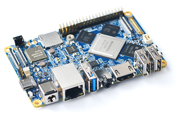
2 Hardware Spec
- SoC: Rockchip RK3399
- CPU: big.LITTLE,Dual-Core Cortex-A72(up to 2.0GHz) + Quad-Core Cortex-A53(up to 1.5GHz)
- GPU: Mali-T864 GPU,supports OpenGL ES1.1/2.0/3.0/3.1, OpenVG1.1, OpenCL, DX11, and AFBC
- VPU: 4K VP9 and 4K 10bits H265/H264 60fps decoding, Dual VOP, etc
- PMU: RK808-D PMIC, cooperated with independent DC/DC, enabling DVFS, solfware power-down, RTC wake-up, system sleep mode
- RAM: Dual-Channel 4GB LPDDR3
- Flash: 16GB eMMC 5.1 Flash
- Ethernet: Native Gigabit Ethernet
- Wi-Fi/BT: 802.11a/b/g/n/ac, Bluetooth 4.1, Wi-Fi and Bluetooth combo module, dual antenna interface
- Video Input: two 4-Lane MIPI-CSI, dual ISP, up to 13MPix/s,supports simultaneous input of dual camera data
- Video output
- HDMI: HDMI 2.0a, supports 4K@60Hz,HDCP 1.4/2.2
- DP on Type-C: DisplayPort 1.2 Alt Mode on USB Type-C
- LCD Interface: one eDP 1.3(4 lane,10.8Gbps), one 4-Lane MIPI-DSI
- Audio Out: 3.5mm Dual channel headphone jack, or HDMI
- Audio In: Onboard microphone
- USB 2.0: 2 independent native USB 2.0 Host A interfaces
- USB 3.0: 1 native USB 3.0 Host A type interface
- USB Type-C: Supports USB3.0 Type-C and DisplayPort 1.2 Alt Mode on USB Type-C
- PCIe: One M.2 M-Key PCIe x4 socket, compatible with PCIe 2.1, Dual operation mode; Onboard M3 PCB nut for mounting M.2 2280 module
- microSD Slot x 1
- 40Pin GPIO Extension ports:
- 1 X 3V/1.8V I2C, up to 2 x 3V UART, 1 X 3V SPI, 1 x SPDIF_TX, up to 8 x 3V GPIOs
- 1 x 1.8V I2S, 3 x 1.8V GPIOs
- ADC: 3 x 1.8V ADC inputs, 5 Pin 2.54mm header
- Debug: one Debug UART, 4 Pin 2.54mm header, 3V level, 1500000bps
- Keys: PowerKey, Reset, MASKROM(BOOT), Recovery
- LED: 1 x power LED and 1 x GPIO Controled LED
- IR reciver: Onboard IR reciver, Acceptes 38KHz carrier frequency
- RTC Battery: 2 Pin 1.27/1.25mm RTC battery input connector
- Cooling: two 2.5mm PCB nuts for mounting heat sink; 3 Pin 12V cooling fan interface with PWM
- Power supply: DC 12V/2A
- PCB: Ten Layer, 100 mm x 64 mm
- Ambient Operating Temperature: 0℃ to 80℃
3 Software Features
4 Diagram, Layout and Dimension
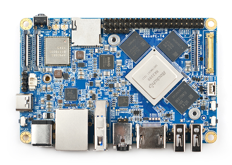
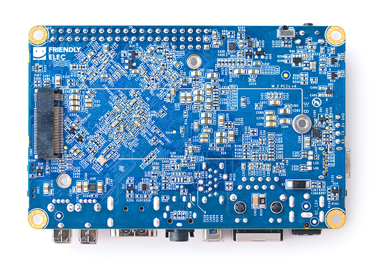
4.1 Layout
File:NanoPC-T4-1802-IF-01.png
NanoPC-T4 Layout
- 40 Pin GPIO Pin Spec
Pin# Assignment Pin# Assignment 1 VCC3V3_SYS 2 VCC5V0_SYS 3 I2C2_SDA(3V) 4 VCC5V0_SYS 5 I2C2_SCL(3V) 6 GND 7 GPIO1_A0(3V) 8 UART2B_TX(3V) 9 GND 10 UART2B_RX(3V) 11 GPIO1_A1(3V) 12 GPIO1_C2(3V) 13 GPIO1_A3(3V) 14 GND 15 GPIO1_A4(3V) 16 GPIO1_C6(3V) 17 VCC3V3_SYS 18 GPIO1_C7(3V) 19 SPI1_TXD/UART4_TX(3V) 20 GND 21 SPI1_RXD/UART4_RX(3V) 22 GPIO1_D0(3V) 23 SPI1_CLK(3V) 24 SPI1_CSn0(3V) 25 GND 26 GPIO4_C5/SPDIF_TX(3V) 27 I2C2_SDA(1.8V) 28 I2C2_SCL(1.8V) 29 I2S1_LRCK_RX(1.8V) 30 GND 31 I2S1_LRCK_TX(1.8V) 32 I2S_CLK(1.8V) 33 I2S1_SCLK(1.8V) 34 GND 35 I2S1_SDI0(1.8V) 36 I2S1_SDO0(1.8V) 37 GPIO3_D4(1.8V) 38 GPIO3_D5(1.8V) 39 GND 40 GPIO3_D6(1.8V)
- eDP Interface Pin Spec
- Connector P/N: I-PEX-20455-030E
Pin# Assignment Description 1 GND Signal ground 2 EDP_TX3N eDP data lane 3 negative output 3 EDP_TX3P eDP data lane 3 positive output 4 GND Signal ground 5 EDP_TX2N eDP data lane 2 negative output 6 EDP_TX2P eDP data lane 2 positive output 7 GND Signal ground 8 EDP_TX1N eDP data lane 1 negative output 9 EDP_TX1P eDP data lane 1 positive output 10 GND Signal ground 11 EDP_TX0N eDP data lane 0 negative output 12 EDP_TX0P eDP data lane 0 positive output 13 GND Signal ground 14 EDPAUXP eDP CH-AUX positive differential output 15 EDPAUXN eDP CH-AUX negative differential output 16 GND Signal ground 17 VCC3V3_SYS 3.3V Power output for logic 18 VCC3V3_SYS 3.3V Power output for logic 19 I2C4_SDA 3V I2C data signal, Connect to touch panel 20 I2C4_SCL 3V I2C clock signal, Connect to touch panel 21 GPIO1_C4_TP_INT 3V interrupt input, Connect to the interrupt output of touch panel 22 GPIO1_B5_TP_RST 3V output for reseting touch panel, Connect to the reset input of touch panel 23 PWM0_BL 3V PWM output, for LCD backlight dimming 24 GPIO4_D5_LCD_BL_EN 3V output for turning on/off the LCD backlight 25 GND Backlight ground 26 GND Backlight ground 27 GND Backlight ground 28 VCC12V0_SYS 12V Power output for Backlight Power 29 VCC12V0_SYS 12V Power output for Backlight Power 30 VCC12V0_SYS 12V Power output for Backlight Power
- MIPI-DSI Interface Pin Spec
- 0.5mm FPC connector
Pin# Assignment Description 1, 2, 3 VCC5V0_SYS 5V power output 4 GND Return current path 5 I2C4_SDA 3V I2C data signal, Connect to touch panel 6 I2C4_SCL 3V I2C clock signal, Connect to touch panel 7 GND Return current path 8 GPIO1_C4_TP_INT 3V interrupt input, Connect to the interrupt output of touch panel 9 GND Return current path 10 PWM0_BL 3V PWM output, for LCD backlight dimming 11 GND Return current path 12 GPIO4_D5_LCD_BL_EN 3V output for turning on/off the LCD backlight 13 GPIO4_D6_LCD_RST_H 3V output for reseting the LCD module 14 GPIO1_B5_TP_RST 3V output for reseting touch panel, Connect to the reset input of touch panel 15 GND Return current path 16 MIPI_TX0_D3N MIPI DSI negative differential data line transceiver output 17 MIPI_TX0_D3P MIPI DSI positive differential data line transceiver output 18 GND Return current path 19 MIPI_TX0_D2N MIPI DSI negative differential data line transceiver output 20 MIPI_TX0_D2P MIPI DSI positive differential data line transceiver output 21 GND Return current path 22 MIPI_TX0_D1N MIPI DSI negative differential data line transceiver output 23 MIPI_TX0_D1P MIPI DSI positive differential data line transceiver output 24 GND Return current path 25 MIPI_TX0_D0N MIPI DSI negative differential data line transceiver output 26 MIPI_TX0_D0P MIPI DSI positive differential data line transceiver output 27 GND Return current path 28 MIPI_TX0_CLKN MIPI DSI negative differential clock line transceiver output 29 MIPI_TX0_CLKP MIPI DSI positive differential clock line transceiver output 30 GND Return current path
- MIPI-CSI Interface Pin Spec
- 0.5mm FPC Connector
Pin# MIPI-CSI1 MIPI-CSI2 Description 1 VCC5V0_SYS VCC5V0_SYS 5V Power ouput 2 VCC5V0_SYS VCC5V0_SYS 5V Power ouput 3 GND GND Return current path 4 VCC_CSI_AF2.8V VCC_CSI_AF2.8V 2.8V Power for VCM 5 VCC_CSI_1.2V VCC_CSI_1.2V 1.2V Power for image sensor core circuit 6 VCC1V8_CAM VCC1V8_CAM 1.8V power for I/O circuit 7 VCC_CSI_2.8V VCC_CSI_2.8V 2.8V power for image sensor analog circuit 8 VCC_CSI_1.0V VCC_CSI_1.0V 1.0V Power for image sensor core circuit 9 I2C1_SCL I2C2_SCL 1.8V I2C clock signal 10 I2C1_SDA I2C2_SDA 1.8V I2C data signal 11 MIPI_CSI0_RST MIPI_CSI1_RST reset camera module 12 MIPI_CSI0_PWN MIPI_CSI1_PWN Power down camera module 13 GND GND Return current path 14 GPIO2_B3_CIF_CLKOUTA GPIO2_B3_CIF_CLKOUTA MCLK to camera module 15 GND GND Return current path 16 MIPI_RX0_D3P MIPI_TX1/RX1_D3P MIPI CSI positive differential data line transceiver output 17 MIPI_RX0_D3N MIPI_TX1/RX1_D3N MIPI CSI negative differential data line transceiver output 18 GND GND Return current path 19 MIPI_RX0_D2P MIPI_TX1/RX1_D2P MIPI CSI positive differential data line transceiver output 20 MIPI_RX0_D2N MIPI_TX1/RX1_D2N MIPI CSI negative differential data line transceiver output 21 GND GND Return current path 22 MIPI_RX0_D1P MIPI_TX1/RX1_D1P MIPI CSI positive differential data line transceiver output 23 MIPI_RX0_D1N MIPI_TX1/RX1_D1N MIPI CSI negative differential data line transceiver output 24 GND GND Return current path 25 MIPI_RX0_CLKP MIPI_TX1/RX1_CLKP MIPI CSI positive differential clock line transceiver output 26 MIPI_RX0_CLKN MIPI_TX1/RX1_CLKN MIPI CSI negative differential clock line transceiver output 27 GND GND Return current path 28 MIPI_RX0_D0P MIPI_TX1/RX1_D0P MIPI CSI positive differential data line transceiver output 29 MIPI_RX0_D0N MIPI_TX1/RX1_D0N MIPI CSI negative differential data line transceiver output 30 GND GND Return current path
- Notes
- VCC5V0_SYS: 5V Output
- VCC3V3_SYS: 3.3V Output
- For more details refer to the document:
4.2 Board Dimension
- For more details refer to the document:
- Power Jack


