Difference between revisions of "SOM-RK3399 Dev Kit"
From FriendlyELEC WiKi
(→Introduction) |
(updated by API) |
||
| (5 intermediate revisions by 2 users not shown) | |||
| Line 12: | Line 12: | ||
==Hardware Spec== | ==Hardware Spec== | ||
| − | * CPU Board: [[SOM-RK3399]], 2GB DDR3,16GB eMMC | + | * CPU Board: [[SOM-RK3399]], 2GB DDR3,16GB eMMC (32/64GB optional) |
* connectivity : | * connectivity : | ||
| − | ** IEEE 802.11b/g/n/AC Wi-Fi | + | ** IEEE 802.11b/g/n/AC 2x2 MIMO, Wi-Fi |
** Bluetooth 4.1 | ** Bluetooth 4.1 | ||
** One 10/100/1000M Ethernet Port | ** One 10/100/1000M Ethernet Port | ||
| Line 558: | Line 558: | ||
| style="font-weight:bold;" | K2 | | style="font-weight:bold;" | K2 | ||
| GPIO1_A3 | | GPIO1_A3 | ||
| − | | | + | | 35 |
| Low | | Low | ||
|- | |- | ||
| Line 574: | Line 574: | ||
| style="font-weight:bold;" | Active | | style="font-weight:bold;" | Active | ||
|- | |- | ||
| − | | style="font-weight:bold;" | | + | | style="font-weight:bold;" | Emerald |
| GPIO1_C7 | | GPIO1_C7 | ||
| 55 | | 55 | ||
| Hight | | Hight | ||
|- | |- | ||
| − | | style="font-weight:bold;" | | + | | style="font-weight:bold;" | Orange |
| GPIO1_D0 | | GPIO1_D0 | ||
| 56 | | 56 | ||
| Line 619: | Line 619: | ||
==Link to Rockchip Resources== | ==Link to Rockchip Resources== | ||
*Link to Rockchip's resources: https://gitlab.com/friendlyelec/rk3399-nougat/tree/nanopc-t4-nougat/RKDocs | *Link to Rockchip's resources: https://gitlab.com/friendlyelec/rk3399-nougat/tree/nanopc-t4-nougat/RKDocs | ||
| − | + | {{Link_to_RK3399_datasheet}} | |
| − | + | ||
==Schematic, PCB CAD File== | ==Schematic, PCB CAD File== | ||
| − | *[http://wiki. | + | *[http://wiki.friendlyelec.com/wiki/images/d/de/SOM-RK3399_Dev_Kit_1904_Schematic.pdf SOM-RK3399_Dev_Kit_1904_Schematic.pdf] |
| − | *[http://wiki. | + | *[http://wiki.friendlyelec.com/wiki/images/7/7f/SOM-RK3399_Dev_Kit_1904_dxf.zip SOM-RK3399_Dev_Kit_1904_dxf.zip] |
Latest revision as of 08:41, 3 June 2024
Contents
1 Introduction
- The SOM-RK3399 is a 260-pin high performance ARM module designed and developed by FriendlyElec. It is based on Rockchip’s 64-bit hexa-core RK3399 SoC. The regular version has 2GB DDR3 RAM, 16GB Flash, onboard 2x2 MIMO dual-antenna WiFi module. Its dimension is 69.6 x 50 mm. It has a TypeC power port and USB-C display port, and can work by itself without a carrier board.
- The SOM-RK3399 module has various interfaces and ports. It can drive a 4-channel NVMe high speed SSD hard disk by working with a carrier board and the read/write rate can reach up to 1GB/s. It can drive dual-MIPI WDR cameras. It has an eDP interface, MIPI interface, USB 3.0, two USB 2.0 interfaces and other interfaces such as I2C, I2S, SPI, PWM, GPIO, serial and etc.
- The SOM-RK3399 can run popular OS systems such as Android 8.1, Ubuntu 18.04, Armbian and Buildroot smoothly. It has well established software support. Especially it has NN SDK packages for neural networks in Android 8.1, VPU hardware encoding/decoding in Qt-5.10, and GPU graphic acceleration. It supports development of dynamic GUI with Qt Quick. It is a perfect platform for startups to develop applications and prototypes in facial detection, machine vision, VR, autonomous-driving, deep learning, AI and etc.
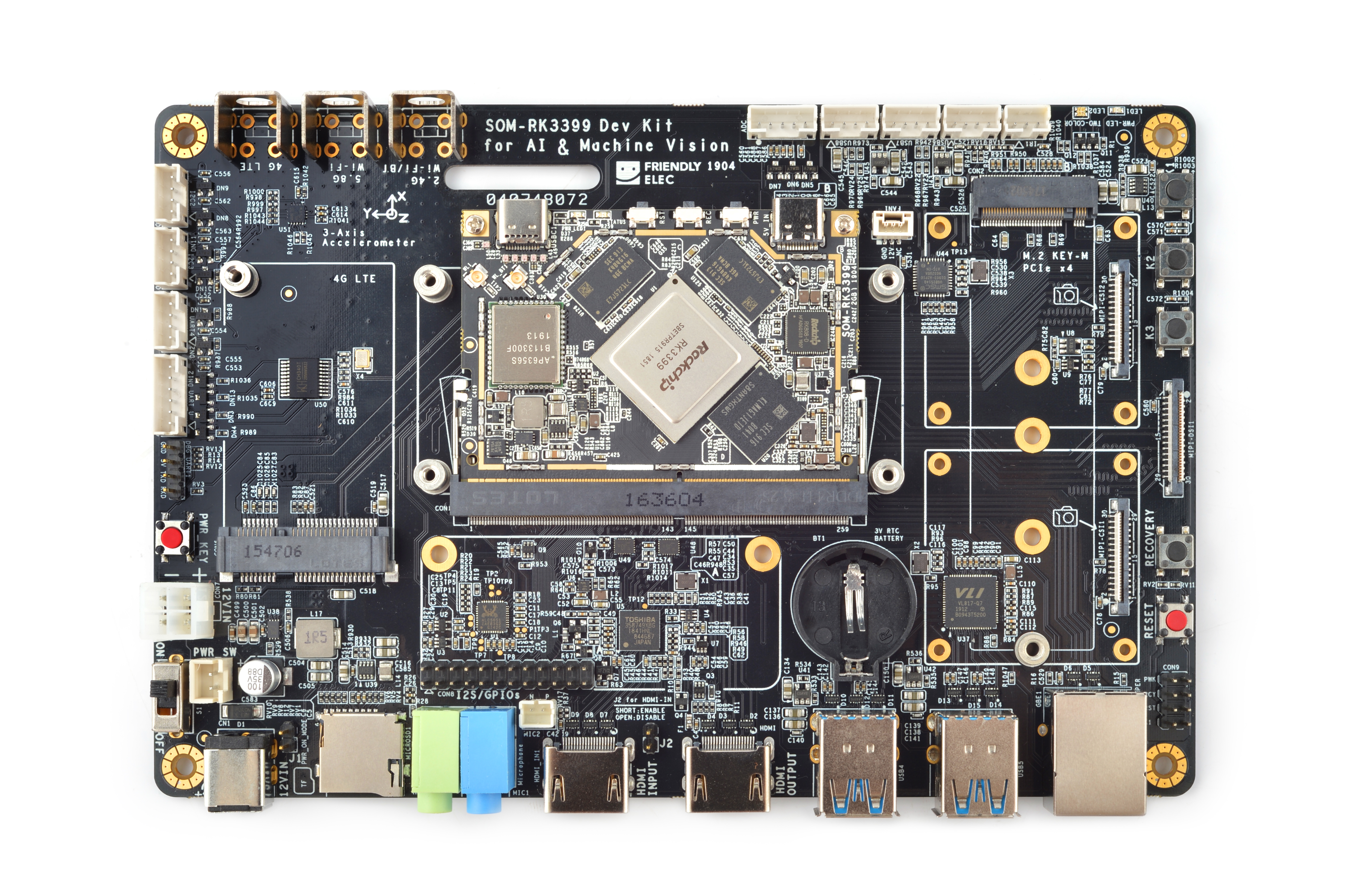
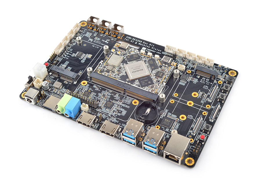
2 Hardware Spec
- CPU Board: SOM-RK3399, 2GB DDR3,16GB eMMC (32/64GB optional)
- connectivity :
- IEEE 802.11b/g/n/AC 2x2 MIMO, Wi-Fi
- Bluetooth 4.1
- One 10/100/1000M Ethernet Port
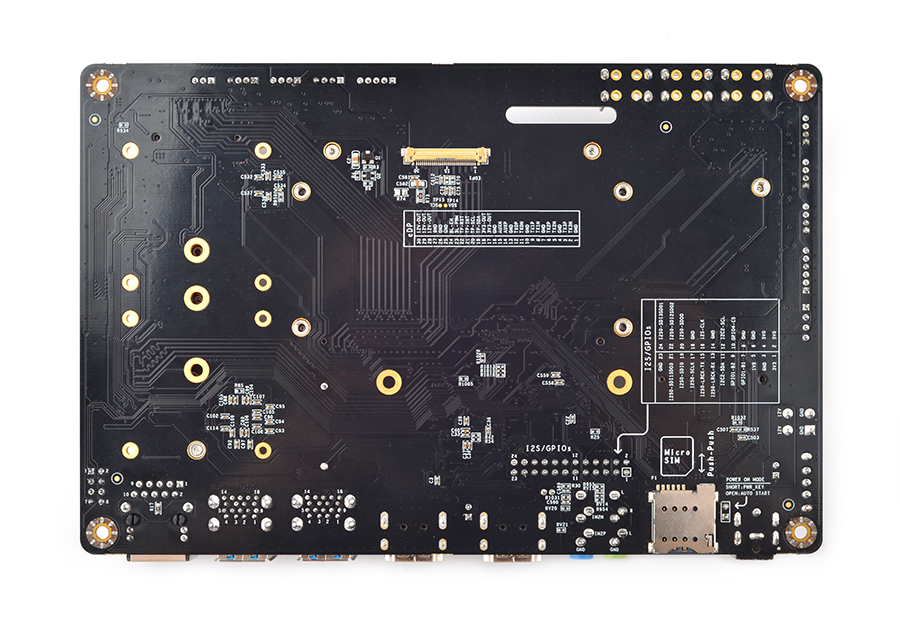
- One MiniPCIe Socket and microSIM slot for 4G LTE module
- USB
- One USB Type-C Port
- 4xUSB3.0 Type-A port
- 3xUSB2.0 PH2.0 connector
- Video out
- One HDMI Type-A, support HDMI 2.0a, supports 4K@60Hz,HDCP 1.4/2.2
- DisplayPort 1.2 Alt Mode on USB Type-C
- one eDP 1.3(4-Lane,10.8Gbps)
- one or two 4-Lane MIPI-DSI
- Video In/Camera interface
- One HDMI IN, support 1080p@30fps, 1280x720@60fps video and audio recording
- one or two 4-Lane MIPI-CSI, up to 13MPix/s,supports simultaneous input of dual camera data
- Audio
- One 3.5mm stereo headphone Jack
- One 3.5mm microphone Jack
- One PH2.0 connector for microphone
- One mciroSD card slot
- One PCIe x4 M.2 Key-M Socket
- Button: PowerKey, Reset, Recovery, 3xUserKey
- LED: One Power LED, One user dual color led
- RTC:CR2032 3V battery holder
- others: 3xADCs,1xIR-IN,2xI2Cs,2xUARTs,1x8ch-I2S,3xGPIOS,1xSPDIF-TX,1x12V cooling fan interface
- Power Supply: DC 12V
- 4-layer PCB
3 Software Features
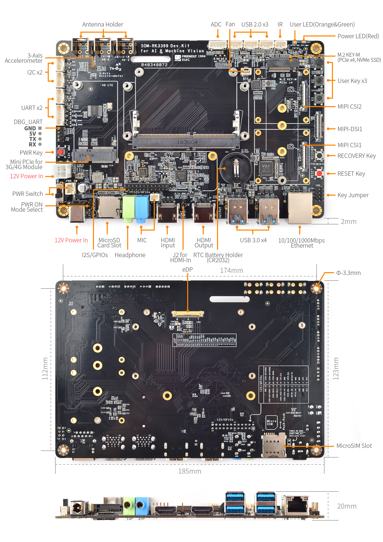
4 Diagram, Layout and Dimension
- HDMI IN
- Short J2 to enable HDMI IN. The HDMI IN and MIPI-CSI1 interfaces cannot be used at the same time.
- MIPI-CSI
- 0.5mm FPC Connector
- MIPI-CSI2 can be configured to MIPI-DSI. To use the MIPI-CSI1 interface, unplug the HDMI cable of the HDMI IN.
Pin# MIPI-CSI1 MIPI-CSI2 Description 1 VCC5V0_SYS VCC5V0_SYS 5V Power ouput 2 VCC5V0_SYS VCC5V0_SYS 5V Power ouput 3 GND GND Return current path 4 VCC_CSI_AF2.8V VCC_CSI_AF2.8V 2.8V Power for VCM 5 VCC_CSI_1.2V VCC_CSI_1.2V 1.2V Power for image sensor core circuit 6 VCC1V8_CAM VCC1V8_CAM 1.8V power for I/O circuit 7 VCC_CSI_2.8V VCC_CSI_2.8V 2.8V power for image sensor analog circuit 8 VCC_CSI_1.0V VCC_CSI_1.0V 1.0V Power for image sensor core circuit 9 I2C1_SCL I2C2_SCL 1.8V I2C clock signal 10 I2C1_SDA I2C2_SDA 1.8V I2C data signal 11 MIPI_CSI0_RST MIPI_CSI1_RST reset camera module 12 MIPI_CSI0_PWN MIPI_CSI1_PWN Power down camera module 13 GND GND Return current path 14 GPIO2_B3_CIF_CLKOUTA GPIO2_B3_CIF_CLKOUTA MCLK to camera module 15 GND GND Return current path 16 MIPI_RX0_D3P MIPI_TX1/RX1_D3P MIPI CSI positive differential data line transceiver output 17 MIPI_RX0_D3N MIPI_TX1/RX1_D3N MIPI CSI negative differential data line transceiver output 18 GND GND Return current path 19 MIPI_RX0_D2P MIPI_TX1/RX1_D2P MIPI CSI positive differential data line transceiver output 20 MIPI_RX0_D2N MIPI_TX1/RX1_D2N MIPI CSI negative differential data line transceiver output 21 GND GND Return current path 22 MIPI_RX0_D1P MIPI_TX1/RX1_D1P MIPI CSI positive differential data line transceiver output 23 MIPI_RX0_D1N MIPI_TX1/RX1_D1N MIPI CSI negative differential data line transceiver output 24 GND GND Return current path 25 MIPI_RX0_CLKP MIPI_TX1/RX1_CLKP MIPI CSI positive differential clock line transceiver output 26 MIPI_RX0_CLKN MIPI_TX1/RX1_CLKN MIPI CSI negative differential clock line transceiver output 27 GND GND Return current path 28 MIPI_RX0_D0P MIPI_TX1/RX1_D0P MIPI CSI positive differential data line transceiver output 29 MIPI_RX0_D0N MIPI_TX1/RX1_D0N MIPI CSI negative differential data line transceiver output 30 GND GND Return current path
- MIPI-DSI
- 0.5mm FPC connector
Pin# Assignment Description 1, 2, 3 VCC5V0_SYS 5V power output 4 GND Return current path 5 I2C4_SDA 3V I2C data signal, Connect to touch panel 6 I2C4_SCL 3V I2C clock signal, Connect to touch panel 7 GND Return current path 8 GPIO1_C4_TP_INT 3V interrupt input, Connect to the interrupt output of touch panel 9 GND Return current path 10 PWM0_BL 3V PWM output, for LCD backlight dimming 11 GND Return current path 12 GPIO4_D5_LCD_BL_EN 3V output for turning on/off the LCD backlight 13 GPIO4_D6_LCD_RST_H 3V output for reseting the LCD module 14 GPIO1_B5_TP_RST 3V output for reseting touch panel, Connect to the reset input of touch panel 15 GND Return current path 16 MIPI_TX0_D3N MIPI DSI negative differential data line transceiver output 17 MIPI_TX0_D3P MIPI DSI positive differential data line transceiver output 18 GND Return current path 19 MIPI_TX0_D2N MIPI DSI negative differential data line transceiver output 20 MIPI_TX0_D2P MIPI DSI positive differential data line transceiver output 21 GND Return current path 22 MIPI_TX0_D1N MIPI DSI negative differential data line transceiver output 23 MIPI_TX0_D1P MIPI DSI positive differential data line transceiver output 24 GND Return current path 25 MIPI_TX0_D0N MIPI DSI negative differential data line transceiver output 26 MIPI_TX0_D0P MIPI DSI positive differential data line transceiver output 27 GND Return current path 28 MIPI_TX0_CLKN MIPI DSI negative differential clock line transceiver output 29 MIPI_TX0_CLKP MIPI DSI positive differential clock line transceiver output 30 GND Return current path
- eDP
- Connector P/N: I-PEX-20455-030E
Pin# Assignment Description 1 GND Signal ground 2 EDP_TX3N eDP data lane 3 negative output 3 EDP_TX3P eDP data lane 3 positive output 4 GND Signal ground 5 EDP_TX2N eDP data lane 2 negative output 6 EDP_TX2P eDP data lane 2 positive output 7 GND Signal ground 8 EDP_TX1N eDP data lane 1 negative output 9 EDP_TX1P eDP data lane 1 positive output 10 GND Signal ground 11 EDP_TX0N eDP data lane 0 negative output 12 EDP_TX0P eDP data lane 0 positive output 13 GND Signal ground 14 EDPAUXP eDP CH-AUX positive differential output 15 EDPAUXN eDP CH-AUX negative differential output 16 GND Signal ground 17 VCC3V3_SYS 3.3V Power output for logic 18 VCC3V3_SYS 3.3V Power output for logic 19 I2C4_SDA 3V I2C data signal, Connect to touch panel 20 I2C4_SCL 3V I2C clock signal, Connect to touch panel 21 GPIO1_C4_TP_INT 3V interrupt input, Connect to the interrupt output of touch panel 22 GPIO1_B5_TP_RST 3V output for reseting touch panel, Connect to the reset input of touch panel 23 PWM0_BL 3V PWM output, for LCD backlight dimming. pull up to VCC3V3_SYS on LCD side. 24 GPIO4_D5_LCD_BL_EN 3V output for turning on/off the LCD backlight 25 GND Backlight ground 26 GND Backlight ground 27 GND Backlight ground 28 VCC12V0_SYS 12V Power output for Backlight Power 29 VCC12V0_SYS 12V Power output for Backlight Power 30 VCC12V0_SYS 12V Power output for Backlight Power
- PCIex4 M.2
- PCIe Gen 2.1 x4
- M.2 Key M Connector for Socket 2/Socket 3 PCIe-based Module, such as PCIe SSD
- Connector P/N: MDT-420-M-01002
Pin# Assignment Description Pin# Assignment Description 1 GND Return current path 2 VCC3V3_SYS 3.3V Power output 3 GND Return current path 4 VCC3V3_SYS 3.3V Power output 5 PCIE_RX3_N PCIe differential data input signals 6 N/C no connection 7 PCIE_RX3_P PCIe differential data input signals 8 N/C no connection 9 GND Return current path 10 N/C no connection 11 PCIE_TX3N PCIe differential data output signals 12 VCC3V3_SYS 3.3V Power output 13 PCIE_TX3P PCIe differential data output signals 14 VCC3V3_SYS 3.3V Power output 15 GND Return current path 16 VCC3V3_SYS 3.3V Power output 17 PCIE_RX2_N PCIe differential data input signals 18 VCC3V3_SYS 3.3V Power output 19 PCIE_RX2_P PCIe differential data input signals 20 N/C no connection 21 GND Return current path 22 N/C no connection 23 PCIE_TX2N PCIe differential data output signals 24 N/C no connection 25 PCIE_TX2P PCIe differential data output signals 26 N/C no connection 27 GND Return current path 28 N/C no connection 29 PCIE_RX1_N PCIe differential data input signals 30 N/C no connection 31 PCIE_RX1_P PCIe differential data input signals 32 N/C no connection 33 GND Return current path 34 N/C no connection 35 PCIE_TX1N PCIe differential data output signals 36 N/C no connection 37 PCIE_TX1P PCIe differential data output signals 38 DEVSLP/NC internal pull up to VCC3V3_SYS with 10K 39 GND Return current path 40 I2C2_SCL 1.8V I2C clock signal 41 PCIE_RX0_N PCIe differential data input signals 42 I2C2_SDA 1.8V I2C data signal 43 PCIE_RX0_P PCIe differential data input signals 44 GPIO2_A2_PCIE_ALERT# 1.8V GPIO signal 45 GND Return current path 46 N/C no connection 47 PCIE_TX0N PCIe differential data output signals 48 N/C no connection 49 PCIE_TX0P PCIe differential data output signals 50 GPIO2_A4_PCIE_RESET# 1.8V GPIO signal 51 GND Return current path 52 CLKREQ#/NC internal pull down to GND with 0R 53 PCIE_REF_CLKN differential reference clock out for PCIe peripheral 54 GPIO2_A3_PCIE_WAKE# 1.8V GPIO signal 55 PCIE_REF_CLKP differential reference clock out for PCIe peripheral 56 N/C no connection 57 GND Return current path 58 N/C no connection 59 Connector Key Connector Key 60 Connector Key Connector Key 60 Connector Key Connector Key 61 Connector Key Connector Key 62 Connector Key Connector Key 63 Connector Key Connector Key 64 Connector Key Connector Key 65 Connector Key Connector Key 66 Connector Key Connector Key 67 N/C no connection 68 RTC_CLKO_SOC 1.8V 32.768KHz clock output 69 N/C no connection 70 VCC3V3_SYS 3.3V Power output 71 GND Return current path 72 VCC3V3_SYS 3.3V Power output 73 GND Return current path 74 VCC3V3_SYS 3.3V Power output 75 GND Return current path
- PH2.0 connectors(USB2.0 I2C, UART, ADC, IR)
- I2C2, I2C3, UART4, and UART_U are 3.3V level; the ADC input range is 0~1.8V; connect IR receiver to the IR IN interface (IR1) directly.
- UART_U is an USB to serial UART.
USB2.0 I2C2,I2C3 UART4 UART_U ADC IR IN Pin# Assignment Pin# Assignment Pin# Assignment Pin# Assignment Pin# Assignment Pin# Assignment 1 5V 1 GND 1 GND 1 GND 1 GND 1 DATA 2 DM 2 SDA 2 RX 2 CTS 2 1.8V out 2 GND 3 DP 3 SCL 3 TX 3 RTS 3 ADC0 3 3.3V 4 GND 4 5V 4 5V 4 RX 4 ADC2 5 TX 5 ADC3 6 5V
- Microphone
- The 3.5mm headphone jack (MIC1) and the PH2.0 connector (MIC2) are the same microphone input. When the 3.5mm headphone jack is inserted, the signal of the PH2.0 connector is disconnected.
- Power Supply
- Two power input connectors, 5.5*2.1 DC socket and 4Pin PC power socket(Molex 5566-04A, or compatible).
- J1 is the power-on mode select jumper. If open, CPU board is automatically turned on when the power is turned on. If short, you need to press the power button to turn the CPU board on.
- Must be powered by a 12V power supply.
- Fan & heatsink
- Connector Model: JST GH Series Connector, 3Pin, BM03B-GHS-TBT
Pin# Assignment Description 1 GND 0V 2 12V 12V output ,controlled by GPIO4_C6/PWM1 3 /NC
- I2S/GPIOs
Pin# Assignment Description Pin# Assignment Description 1 VCC3V3_SYS 3.3V Power Output, 500mA MAX 2 VCC5V0_SYS 5V Power Output, 2A MAX 3 VCC_1V8 1.8V Power Output,100mA MAX 4 VCC5V0_SYS 5V Power Output, 2A MAX 5 GND System Ground(0V) 6 GND System Ground(0V) 7 GPIO1_B1 3V GPIO. Linux GPIO 41 8 GND System Ground(0V) 9 GPIO1_B2 3V GPIO. Linux GPIO 42 10 GPIO4_C5/SPDIF_TX 3V GPIO. Linux GPIO 149, or SPDIF Output 11 I2C2_SDA I2C2 data, 1.8V level, open drian with 2.2K pulled internal 12 I2C2_SCL I2C2 clock, 1.8V level, open drian with 2.2K pulled internal 13 I2S0_LRCK_RX I2S0 word select for input data, 1.8V level 14 GND System Ground(0V) 15 I2S0_LRCK_TX I2S0 word select for output data, 1.8V level 16 I2S_CLK I2S Mclk for I2S0 and I2S1 17 I2S0_SCLK I2S0 continuous serial clock, 1.8V level 18 GND System Ground(0V) 19 I2S0_SDI0 I2S0 serial data, 1.8V level 20 I2S0_SDO0 I2S0 serial data, 1.8V level 21 I2S0_SDI1SDO3 I2S0 serial data, 1.8V level 22 I2S0_SDI2SDO2 I2S0 serial data, 1.8V level 23 GND System Ground(0V) 24 I2S0_SDI3SDO1 I2S0 serial data, 1.8V level
- LED & Button
Key# GPIO Linux GPIO Active Note K1 GPIO1_A1 33 Low GPIO is suspended by default, RK3399 internal pull-up must be enabled K2 GPIO1_A3 35 Low K3 GPIO1_A4 36 Low
Two-color LED (LED2) Color GPIO Linux GPIO Active Emerald GPIO1_C7 55 Hight Orange GPIO1_D0 56 Hight
- Button Jumper(CON9)
Pin# Assignment Pin# Assignment Description 1 PWR_KEY 2 GND for power button 3 RECOVERY 4 GND for RECOVERY button 5 RESET_IN_H 6 VCC3V3_SYS for reset button 7 KEY1 8 GND for K1
5 Link to Rockchip Resources
- Link to Rockchip's resources: https://gitlab.com/friendlyelec/rk3399-nougat/tree/nanopc-t4-nougat/RKDocs
- RK3399 datasheet V2.1
- RK3399TRM V1.4


