Difference between revisions of "Power Dock for NanoPi NEO"
From FriendlyELEC WiKi
(Created page with "查看中文") |
|||
| Line 1: | Line 1: | ||
[[Power Dock for NanoPi NEO/zh|查看中文]] | [[Power Dock for NanoPi NEO/zh|查看中文]] | ||
| + | |||
| + | ==Introduction== | ||
| + | [[File:Power Dock for NanoPi NEO .png|thumb|Power Dock for NanoPi NEO]] | ||
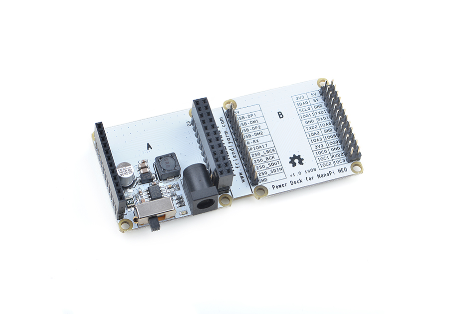
| + | * The Power Dock for NanoPi NEO is a power conversion board. | ||
| + | * It uses TI's TPS54331 device with wide voltage range. | ||
| + | <!---with an integrated high-side n-channel | ||
| + | MOSFET. To improve performance during line and load transients, the device implements a constant-frequency, | ||
| + | current mode control which reduces output capacitance and simplifies external frequency compensation design. | ||
| + | The TPS54331 device has a preset switching frequency of 570 kHz. | ||
| + | , .电源转换芯片,输入电压范围宽,带载能力强,输出电流大。使用了低内阻、大电流屏蔽电感,提高转换效率,降低发热量。---> | ||
| + | * Its slow-start feature limits inrush currents. Its overvoltage transient protection circuit limits voltage overshoots during startup and transient conditions. | ||
| + | * Its side A has double-layer tall female connectors which allow a NEO to be stacked on the board. Its side B populates NEO's GPIO pins. | ||
| + | |||
| + | ==Hardware Spec== | ||
| + | * Input Voltage: 12V | ||
| + | * Output: 5V/2A | ||
| + | * Switching Frequency: 570KHz | ||
| + | * Shutdown Quiescent Current: 1uA | ||
| + | <!---* 输入欠压保护---> | ||
| + | * Overvoltage Protection | ||
| + | * Slow-Start | ||
| + | <!--- | ||
| + | * 负载调整率:±1% | ||
| + | * 电压调整率:±0.5% | ||
| + | ---> | ||
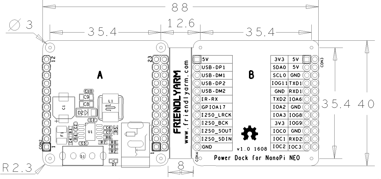
| + | * PCB dimension(mm): 40 x 88 | ||
| + | [[File:Power Dock for NanoPi NEO.png | frameless|800px|Power Dock for NanoPi NEO_PCB]] | ||
| + | |||
| + | * Pin Description: | ||
| + | * '''GPIO Pin Description''' | ||
| + | {| class="wikitable" | ||
| + | |- | ||
| + | |Pin# || Name || Linux gpio ||Pin# || Name || Linux gpio | ||
| + | |- | ||
| + | |1 || SYS_3.3V || ||2 || VDD_5V || | ||
| + | |- | ||
| + | |3 || I2C0_SDA || ||4 || VDD_5V || | ||
| + | |- | ||
| + | |5 || I2C0_SCL || ||6 || GND || | ||
| + | |- | ||
| + | |7 || GPIOG11 || 203 ||8 || UART1_TX/GPIOG6 || 198 | ||
| + | |- | ||
| + | |9 || GND || ||10 || UART1_RX/GPIOG7 || 199 | ||
| + | |- | ||
| + | |11 || UART2_TX/GPIOA0 || 0 ||12 || PWM1/GPIOA6 || 6 | ||
| + | |- | ||
| + | |13 || UART2_RTS/GPIOA2 || 2 ||14 || GND || | ||
| + | |- | ||
| + | |15 || UART2_CTS/GPIOA3 || 3 ||16 || UART1_RTS/GPIOG8 || 200 | ||
| + | |- | ||
| + | |17 || SYS_3.3V || ||18 || UART1_CTS/GPIOG9 || 201 | ||
| + | |- | ||
| + | |19 || SPI0_MOSI/GPIOC0 || 64 ||20 || GND || | ||
| + | |- | ||
| + | |21 || SPI0_MISO/GPIOC1 || 65 ||22 || UART2_RX/GPIOA1 || 1 | ||
| + | |- | ||
| + | |23 || SPI0_CLK/GPIOC2 || 93 ||24 || SPI0_CS/GPIOC3 || 67 | ||
| + | |} | ||
| + | |||
| + | * '''USB/Audio/IR Pin Description''' | ||
| + | {| class="wikitable" | ||
| + | |- | ||
| + | | style="background: PaleTurquoise; color: black" colspan="3"| '''NanoPi-NEO V1.1''' | ||
| + | |- | ||
| + | |Pin# || Name || Description | ||
| + | |- | ||
| + | |1 || VDD_5V || 5V Power Out | ||
| + | |- | ||
| + | |2 || USB-DP1 || USB1 DP Signal | ||
| + | |- | ||
| + | |3 || USB-DM1 || USB1 DM Signal | ||
| + | |- | ||
| + | |4 || USB-DP2 || USB2 DP Signal | ||
| + | |- | ||
| + | |5 || USB-DM2 || USB2 DM Signal | ||
| + | |- | ||
| + | |6 || GPIOL11/IR-RX || GPIOL11 or IR Receive | ||
| + | |- | ||
| + | |7 || SPDIF-OUT/GPIOA17 || GPIOA17 or SPDIF-OUT | ||
| + | |- | ||
| + | |8 || PCM0_SYNC/I2S0_LRC || I2S/PCM Sample Rate Clock/Sync | ||
| + | |- | ||
| + | |9 || PCM0_CLK/I2S0_BCK || I2S/PCM Sample Rate Clock | ||
| + | |- | ||
| + | |10 || PCM0_DOUT/I2S0_SDOUT || I2S/PCM Serial Bata Output | ||
| + | |- | ||
| + | |11 || PCM0_DIN/I2S0_SDIN || I2S/PCM Serial Data Input | ||
| + | |- | ||
| + | |12 || GND || 0V | ||
| + | |} | ||
| + | |||
| + | ==Device Operation== | ||
| + | *The Power Dock for NanoPi NEO uses TI's TPS54331 device. The TPS54331 device is a 28-V, 3-A non-synchronous buck converter that integrates a low RDS(on) high-side MOSFET. | ||
| + | |||
| + | ==Hardware Setup== | ||
| + | ===Connect Power Dock to NanoPi NEO=== | ||
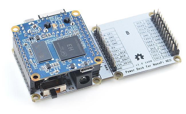
| + | A NanoPi NEO can be stacked on the board at side A's female connector. Its side B populates NEO's GPIO pins.<br> | ||
| + | |||
| + | Hardware Setup<br> | ||
| + | [[File:Power Dock for NanoPi NEO_nanopi_NEO.jpg|frameless|500px|Power Dock for NanoPi NEO_nanopi_NEO]]<br> | ||
| + | Connect Power Dock to NanoPi BAT & Other Modules:<br> | ||
| + | [[File:Power Dock for NanoPi NEO_nanopi_NEO0.jpg|frameless|400px|Power Dock for NanoPi BAT]] | ||
| + | [[File:Power Dock for NanoPi NEO_nanopi_NEO1.jpg|frameless|400px|Power Dock for NanoPi NEO Hub]] | ||
| + | [[File:Power Dock for NanoPi NEO_nanopi_NEO2.jpg|frameless|400px|Power Dock for NanoPi RTC]] | ||
| + | [[File:Power Dock for NanoPi NEO_nanopi_NEO3.jpg|frameless|400px|Power Dock for NanoPi GPS]] | ||
| + | |||
| + | ==Resources== | ||
Revision as of 16:55, 18 April 2017
Contents
[hide]1 Introduction
- The Power Dock for NanoPi NEO is a power conversion board.
- It uses TI's TPS54331 device with wide voltage range.
- Its slow-start feature limits inrush currents. Its overvoltage transient protection circuit limits voltage overshoots during startup and transient conditions.
- Its side A has double-layer tall female connectors which allow a NEO to be stacked on the board. Its side B populates NEO's GPIO pins.
2 Hardware Spec
- Input Voltage: 12V
- Output: 5V/2A
- Switching Frequency: 570KHz
- Shutdown Quiescent Current: 1uA
- Overvoltage Protection
- Slow-Start
- PCB dimension(mm): 40 x 88
- Pin Description:
- GPIO Pin Description
| Pin# | Name | Linux gpio | Pin# | Name | Linux gpio |
| 1 | SYS_3.3V | 2 | VDD_5V | ||
| 3 | I2C0_SDA | 4 | VDD_5V | ||
| 5 | I2C0_SCL | 6 | GND | ||
| 7 | GPIOG11 | 203 | 8 | UART1_TX/GPIOG6 | 198 |
| 9 | GND | 10 | UART1_RX/GPIOG7 | 199 | |
| 11 | UART2_TX/GPIOA0 | 0 | 12 | PWM1/GPIOA6 | 6 |
| 13 | UART2_RTS/GPIOA2 | 2 | 14 | GND | |
| 15 | UART2_CTS/GPIOA3 | 3 | 16 | UART1_RTS/GPIOG8 | 200 |
| 17 | SYS_3.3V | 18 | UART1_CTS/GPIOG9 | 201 | |
| 19 | SPI0_MOSI/GPIOC0 | 64 | 20 | GND | |
| 21 | SPI0_MISO/GPIOC1 | 65 | 22 | UART2_RX/GPIOA1 | 1 |
| 23 | SPI0_CLK/GPIOC2 | 93 | 24 | SPI0_CS/GPIOC3 | 67 |
- USB/Audio/IR Pin Description
| NanoPi-NEO V1.1 | ||
| Pin# | Name | Description |
| 1 | VDD_5V | 5V Power Out |
| 2 | USB-DP1 | USB1 DP Signal |
| 3 | USB-DM1 | USB1 DM Signal |
| 4 | USB-DP2 | USB2 DP Signal |
| 5 | USB-DM2 | USB2 DM Signal |
| 6 | GPIOL11/IR-RX | GPIOL11 or IR Receive |
| 7 | SPDIF-OUT/GPIOA17 | GPIOA17 or SPDIF-OUT |
| 8 | PCM0_SYNC/I2S0_LRC | I2S/PCM Sample Rate Clock/Sync |
| 9 | PCM0_CLK/I2S0_BCK | I2S/PCM Sample Rate Clock |
| 10 | PCM0_DOUT/I2S0_SDOUT | I2S/PCM Serial Bata Output |
| 11 | PCM0_DIN/I2S0_SDIN | I2S/PCM Serial Data Input |
| 12 | GND | 0V |
3 Device Operation
- The Power Dock for NanoPi NEO uses TI's TPS54331 device. The TPS54331 device is a 28-V, 3-A non-synchronous buck converter that integrates a low RDS(on) high-side MOSFET.
4 Hardware Setup
4.1 Connect Power Dock to NanoPi NEO
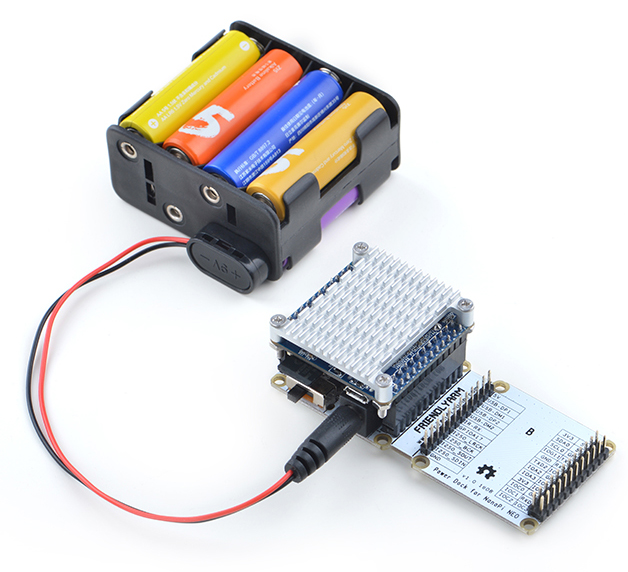
A NanoPi NEO can be stacked on the board at side A's female connector. Its side B populates NEO's GPIO pins.
Hardware Setup
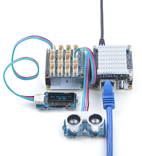
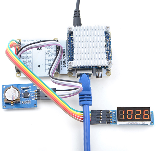
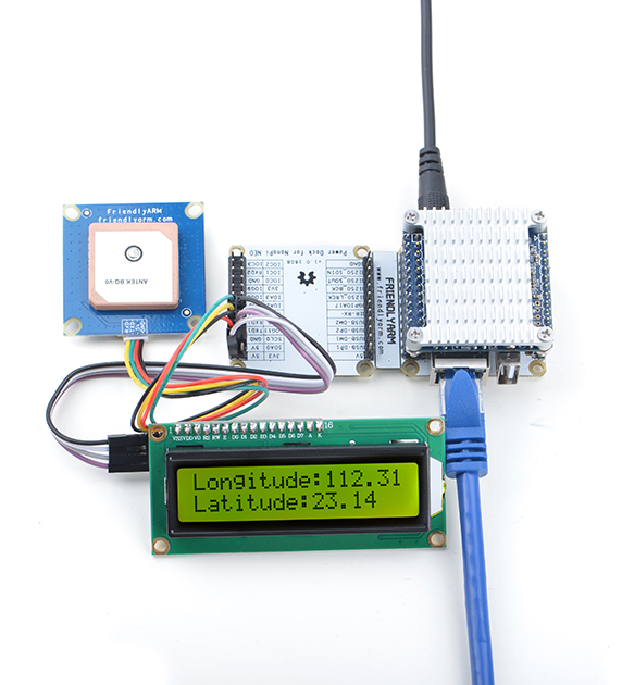
Connect Power Dock to NanoPi BAT & Other Modules:
