NanoPC-T4
Contents
1 Introduction


- The NanoPC-T4 is by far the smallest RK3399 based high-performance ARM board with popular ports and interfaces. Its software is fully open source. It is as small as 100 x 64 mm. It has 4GB LPDDR3 RAM, 16GB eMMC flash, onboard 2.4G & 5G dual-band WiFi module and a full standard M.2 PCIe interface which supports an NVME SSD high-speed hard drive. The NanoPC-T4 supports GPU and VPU acceleration and works with Android 7.1 and Lubuntu Desktop.
- The NanoPC-T4 has a MIPI-CSI dual camera interface, a MIPI-DSI and an eDP display interfaces, and an HDMI 2.0 interface. It has Type-C/DP, USB 3.0, USB2.0, MicroSD, Gbps Ethernet port, 3.5mm audio jack, infrared receiver, AD input, serial debug interface and a 40Pin RPi compatible connector.
- The RK3399 SoC has an internal Mali-T860 GPU which has powerful capabilities of processing 3D and HD H.265/H2.64 video streams. It supports dual camera inputs, dual ISP interface capable of doing image processing up to 13MPix/s. The NanoPC-T4 is a perfect platform for AI and deep learning applications. It can be widely used in advertisement machines, game machines, video conference applications, surveillance systems, clusters, VR/AR applications, machine vision applications and etc.
2 Hardware Spec
- SoC: Rockchip RK3399
- CPU: big.LITTLE,Dual-Core Cortex-A72(up to 2.0GHz) + Quad-Core Cortex-A53(up to 1.5GHz)
- GPU: Mali-T864 GPU,supports OpenGL ES1.1/2.0/3.0/3.1, OpenVG1.1, OpenCL, DX11, and AFBC
- VPU: 4K VP9 and 4K 10bits H265/H264 60fps decoding, Dual VOP, etc
- PMU: RK808-D PMIC, cooperated with independent DC/DC, enabling DVFS, solfware power-down, RTC wake-up, system sleep mode
- RAM: Dual-Channel 4GB LPDDR3-1866
- Flash: 16GB eMMC 5.1 Flash
- Ethernet: Native Gigabit Ethernet
- Wi-Fi/BT: 802.11a/b/g/n/ac, Bluetooth 4.1, Wi-Fi and Bluetooth combo module, dual antenna interface
- Video Input: one or two 4-Lane MIPI-CSI, dual ISP, up to 13MPix/s,supports simultaneous input of dual camera data
- Video output
- HDMI: HDMI 2.0a, supports 4K@60Hz,HDCP 1.4/2.2
- DP on Type-C: DisplayPort 1.2 Alt Mode on USB Type-C
- LCD Interface: one eDP 1.3(4-Lane,10.8Gbps), one or two 4-Lane MIPI-DSI
- Audio Out: 3.5mm Dual channel headphone jack, or HDMI
- Audio In: Onboard microphone
- USB 2.0: 2 independent native USB 2.0 Host A interfaces
- USB 3.0: 1 native USB 3.0 Host A type interface
- USB Type-C: Supports USB3.0 Type-C and DisplayPort 1.2 Alt Mode on USB Type-C
- PCIe: One M.2 M-Key PCIe x4 socket, compatible with PCIe 2.1, Dual operation mode; Onboard M3 PCB nut for mounting M.2 2280 module
- microSD Slot x 1
- 40Pin GPIO Extension ports:
- 1 X 3V/1.8V I2C, up to 2 x 3V UART, 1 X 3V SPI, 1 x SPDIF_TX, up to 8 x 3V GPIOs
- 1 x 1.8V I2S, 3 x 1.8V GPIOs
- ADC: 3 x 1.8V ADC inputs, 5 Pin 2.54mm header
- Debug: one Debug UART, 4 Pin 2.54mm header, 3V level, 1500000bps
- Keys: PowerKey, Reset, MASKROM(BOOT), Recovery
- LED: 1 x power LED and 1 x GPIO Controlled LED
- IR reciver: Onboard IR reciver, Acceptes 38KHz carrier frequency
- RTC Battery: 2 Pin 1.27/1.25mm RTC battery input connector
- Cooling: two 2.5mm PCB nuts for mounting heat sink; 3 Pin 12V cooling fan interface with PWM
- Power supply: DC 12V/2A
- PCB: Ten Layer, 100 mm x 64 mm
- Ambient Operating Temperature: 0℃ to 80℃
3 Software Features
4 Diagram, Layout and Dimension
4.1 Layout

- 40 Pin GPIO Pin Spec
Pin# Assignment Pin# Assignment 1 VCC3V3_SYS 2 VCC5V0_SYS 3 I2C2_SDA(3V) 4 VCC5V0_SYS 5 I2C2_SCL(3V) 6 GND 7 GPIO1_A0(3V) 8 UART2B_TX(3V) 9 GND 10 UART2B_RX(3V) 11 GPIO1_A1(3V) 12 GPIO1_C2(3V) 13 GPIO1_A3(3V) 14 GND 15 GPIO1_A4(3V) 16 GPIO1_C6(3V) 17 VCC3V3_SYS 18 GPIO1_C7(3V) 19 SPI1_TXD/UART4_TX(3V) 20 GND 21 SPI1_RXD/UART4_RX(3V) 22 GPIO1_D0(3V) 23 SPI1_CLK(3V) 24 SPI1_CSn0(3V) 25 GND 26 GPIO4_C5/SPDIF_TX(3V) 27 I2C2_SDA(1.8V) 28 I2C2_SCL(1.8V) 29 I2S1_LRCK_RX(1.8V) 30 GND 31 I2S1_LRCK_TX(1.8V) 32 I2S_CLK(1.8V) 33 I2S1_SCLK(1.8V) 34 GND 35 I2S1_SDI0(1.8V) 36 I2S1_SDO0(1.8V) 37 GPIO3_D4(1.8V) 38 GPIO3_D5(1.8V) 39 GND 40 GPIO3_D6(1.8V)
- eDP Interface Pin Spec
- Connector P/N: I-PEX-20455-030E
Pin# Assignment Description 1 GND Signal ground 2 EDP_TX3N eDP data lane 3 negative output 3 EDP_TX3P eDP data lane 3 positive output 4 GND Signal ground 5 EDP_TX2N eDP data lane 2 negative output 6 EDP_TX2P eDP data lane 2 positive output 7 GND Signal ground 8 EDP_TX1N eDP data lane 1 negative output 9 EDP_TX1P eDP data lane 1 positive output 10 GND Signal ground 11 EDP_TX0N eDP data lane 0 negative output 12 EDP_TX0P eDP data lane 0 positive output 13 GND Signal ground 14 EDPAUXP eDP CH-AUX positive differential output 15 EDPAUXN eDP CH-AUX negative differential output 16 GND Signal ground 17 VCC3V3_SYS 3.3V Power output for logic 18 VCC3V3_SYS 3.3V Power output for logic 19 I2C4_SDA 3V I2C data signal, Connect to touch panel 20 I2C4_SCL 3V I2C clock signal, Connect to touch panel 21 GPIO1_C4_TP_INT 3V interrupt input, Connect to the interrupt output of touch panel 22 GPIO1_B5_TP_RST 3V output for reseting touch panel, Connect to the reset input of touch panel 23 PWM0_BL 3V PWM output, for LCD backlight dimming 24 GPIO4_D5_LCD_BL_EN 3V output for turning on/off the LCD backlight 25 GND Backlight ground 26 GND Backlight ground 27 GND Backlight ground 28 VCC12V0_SYS 12V Power output for Backlight Power 29 VCC12V0_SYS 12V Power output for Backlight Power 30 VCC12V0_SYS 12V Power output for Backlight Power
- MIPI-DSI Interface Pin Spec
- 0.5mm FPC connector
Pin# Assignment Description 1, 2, 3 VCC5V0_SYS 5V power output 4 GND Return current path 5 I2C4_SDA 3V I2C data signal, Connect to touch panel 6 I2C4_SCL 3V I2C clock signal, Connect to touch panel 7 GND Return current path 8 GPIO1_C4_TP_INT 3V interrupt input, Connect to the interrupt output of touch panel 9 GND Return current path 10 PWM0_BL 3V PWM output, for LCD backlight dimming 11 GND Return current path 12 GPIO4_D5_LCD_BL_EN 3V output for turning on/off the LCD backlight 13 GPIO4_D6_LCD_RST_H 3V output for reseting the LCD module 14 GPIO1_B5_TP_RST 3V output for reseting touch panel, Connect to the reset input of touch panel 15 GND Return current path 16 MIPI_TX0_D3N MIPI DSI negative differential data line transceiver output 17 MIPI_TX0_D3P MIPI DSI positive differential data line transceiver output 18 GND Return current path 19 MIPI_TX0_D2N MIPI DSI negative differential data line transceiver output 20 MIPI_TX0_D2P MIPI DSI positive differential data line transceiver output 21 GND Return current path 22 MIPI_TX0_D1N MIPI DSI negative differential data line transceiver output 23 MIPI_TX0_D1P MIPI DSI positive differential data line transceiver output 24 GND Return current path 25 MIPI_TX0_D0N MIPI DSI negative differential data line transceiver output 26 MIPI_TX0_D0P MIPI DSI positive differential data line transceiver output 27 GND Return current path 28 MIPI_TX0_CLKN MIPI DSI negative differential clock line transceiver output 29 MIPI_TX0_CLKP MIPI DSI positive differential clock line transceiver output 30 GND Return current path
- MIPI-CSI Interface Pin Spec
- 0.5mm FPC Connector
- MIPI-CSI2 can be configured to MIPI-DSI
Pin# MIPI-CSI1 MIPI-CSI2 Description 1 VCC5V0_SYS VCC5V0_SYS 5V Power ouput 2 VCC5V0_SYS VCC5V0_SYS 5V Power ouput 3 GND GND Return current path 4 VCC_CSI_AF2.8V VCC_CSI_AF2.8V 2.8V Power for VCM 5 VCC_CSI_1.2V VCC_CSI_1.2V 1.2V Power for image sensor core circuit 6 VCC1V8_CAM VCC1V8_CAM 1.8V power for I/O circuit 7 VCC_CSI_2.8V VCC_CSI_2.8V 2.8V power for image sensor analog circuit 8 VCC_CSI_1.0V VCC_CSI_1.0V 1.0V Power for image sensor core circuit 9 I2C1_SCL I2C2_SCL 1.8V I2C clock signal 10 I2C1_SDA I2C2_SDA 1.8V I2C data signal 11 MIPI_CSI0_RST MIPI_CSI1_RST reset camera module 12 MIPI_CSI0_PWN MIPI_CSI1_PWN Power down camera module 13 GND GND Return current path 14 GPIO2_B3_CIF_CLKOUTA GPIO2_B3_CIF_CLKOUTA MCLK to camera module 15 GND GND Return current path 16 MIPI_RX0_D3P MIPI_TX1/RX1_D3P MIPI CSI positive differential data line transceiver output 17 MIPI_RX0_D3N MIPI_TX1/RX1_D3N MIPI CSI negative differential data line transceiver output 18 GND GND Return current path 19 MIPI_RX0_D2P MIPI_TX1/RX1_D2P MIPI CSI positive differential data line transceiver output 20 MIPI_RX0_D2N MIPI_TX1/RX1_D2N MIPI CSI negative differential data line transceiver output 21 GND GND Return current path 22 MIPI_RX0_D1P MIPI_TX1/RX1_D1P MIPI CSI positive differential data line transceiver output 23 MIPI_RX0_D1N MIPI_TX1/RX1_D1N MIPI CSI negative differential data line transceiver output 24 GND GND Return current path 25 MIPI_RX0_CLKP MIPI_TX1/RX1_CLKP MIPI CSI positive differential clock line transceiver output 26 MIPI_RX0_CLKN MIPI_TX1/RX1_CLKN MIPI CSI negative differential clock line transceiver output 27 GND GND Return current path 28 MIPI_RX0_D0P MIPI_TX1/RX1_D0P MIPI CSI positive differential data line transceiver output 29 MIPI_RX0_D0N MIPI_TX1/RX1_D0N MIPI CSI negative differential data line transceiver output 30 GND GND Return current path
- M.2 PCIe Pin Spec
- PCIe Gen 2.1 x4
- M.2 Key M Connector for Socket 2/Socket 3 PCIe-based Module, such as PCIe SSD
- Connector P/N: MDT-420-M-01002
Pin# Assignment Description Pin# Assignment Description 1 GND Return current path 2 VCC3V3_SYS 3.3V Power output 3 GND Return current path 4 VCC3V3_SYS 3.3V Power output 5 PCIE_RX3_N PCIe differential data input signals 6 N/C no connection 7 PCIE_RX3_P PCIe differential data input signals 8 N/C no connection 9 GND Return current path 10 N/C no connection 11 PCIE_TX3N PCIe differential data output signals 12 VCC3V3_SYS 3.3V Power output 13 PCIE_TX3P PCIe differential data output signals 14 VCC3V3_SYS 3.3V Power output 15 GND Return current path 16 VCC3V3_SYS 3.3V Power output 17 PCIE_RX2_N PCIe differential data input signals 18 VCC3V3_SYS 3.3V Power output 19 PCIE_RX2_P PCIe differential data input signals 20 N/C no connection 21 GND Return current path 22 N/C no connection 23 PCIE_TX2N PCIe differential data output signals 24 N/C no connection 25 PCIE_TX2P PCIe differential data output signals 26 N/C no connection 27 GND Return current path 28 N/C no connection 29 PCIE_RX1_N PCIe differential data input signals 30 N/C no connection 31 PCIE_RX1_P PCIe differential data input signals 32 N/C no connection 33 GND Return current path 34 N/C no connection 35 PCIE_TX1N PCIe differential data output signals 36 N/C no connection 37 PCIE_TX1P PCIe differential data output signals 38 DEVSLP/NC internal pull up to VCC3V3_SYS with 10K 39 GND Return current path 40 I2C2_SCL 1.8V I2C clock signal 41 PCIE_RX0_N PCIe differential data input signals 42 I2C2_SDA 1.8V I2C data signal 43 PCIE_RX0_P PCIe differential data input signals 44 GPIO2_A2_PCIE_ALERT# 1.8V GPIO signal 45 GND Return current path 46 N/C no connection 47 PCIE_TX0N PCIe differential data output signals 48 N/C no connection 49 PCIE_TX0P PCIe differential data output signals 50 GPIO2_A4_PCIE_RESET# 1.8V GPIO signal 51 GND Return current path 52 CLKREQ#/NC internal pull down to GND with 0R 53 PCIE_REF_CLKN differential reference clock out for PCIe peripheral 54 GPIO2_A3_PCIE_WAKE# 1.8V GPIO signal 55 PCIE_REF_CLKP differential reference clock out for PCIe peripheral 56 N/C no connection 57 GND Return current path 58 N/C no connection 59 Connector Key Connector Key 60 Connector Key Connector Key 60 Connector Key Connector Key 61 Connector Key Connector Key 62 Connector Key Connector Key 63 Connector Key Connector Key 64 Connector Key Connector Key 65 Connector Key Connector Key 66 Connector Key Connector Key 67 N/C no connection 68 RTC_CLKO_SOC 1.8V 32.768KHz clock output 69 N/C no connection 70 VCC3V3_SYS 3.3V Power output 71 GND Return current path 72 VCC3V3_SYS 3.3V Power output 73 GND Return current path 74 VCC3V3_SYS 3.3V Power output 75 GND Return current path
- ADC interface Pin Spec
- ADC input rang : 0~1.8V
Pin# Assignment 1 GND 2 VCC_1V8 3 ADC_IN0 4 ADC_IN2 5 ADC_IN3
- Cooling Fan interface Pin Spec
- Connector P/N: BM03B-GHS-TBT
Pin# Assignment Description 1 GND 0V 2 12V 12V output ,controlled by GPIO4_C6/PWM1 3 GPIO2_A6_FAN_TACH connect to tachometer output signal , or float
- Debug UART Pin Spec
- 3V level signals, 1500000bps
Pin# Assignment Description 1 GND 0V 2 VCC5V0_SYS 5V power output 3 UART2DBG_TX output 4 UART2DBG_RX intput
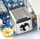
- Power Jack
- DC-12V/2A IN, 5.5*2.1mm Power Jack

- Power Key
- Plug in 12V power at power jack, then press the Power Key ( > 0.5s ) to boot NanoPC-T4.
- USB Port
- USB Type-C port has 2A overcurrent protection.
- USB 3.0 port has 2A overcurrent protection.
- Two USB 2.0 host port share 2A overcurrent protection.
- BOOT Key
- Press BOOT key to prevent the board from eMMC booting, making the board enter MASKROM mode.
- RTC
- RTC backup current is 27uA.
- Notes
- The Power Jack is the only power input port. All power pins at other ports are output.
- How to make T4 start automatically when power is plugged in
- For more details refer to the document: NanoPC-T4-1802-Schematic.pdf
4.2 Board Dimension

- For more details refer to the CAD document: NanoPC-T4_1802_Drawing(dxf).zip
5 Get Started
5.1 Essentials You Need
Before starting to use your NanoPC-T4 get the following items ready
- NanoPC-T4
- Type-C cable
- TF Card: Class 10 or Above, minimum 8GB SDHC
- USB to serial(optinal, for debugging or access from PC host)
- A DC 12V/2A power is a must
- HDMI monitor or LCD
- USB keyboard, mouse and possible a USB hub(or a TTL to serial board)
- A host computer running Ubuntu 14.04 64 bit system or Windows 7
5.2 Debug with Serial Pins
如果你想查看NanoPC-T4启动时更多详细的信息,或者更直接的对其进行控制,建议连接并使用调试串口。
- 使用准备好的USB转串口适配器和连接线(需另购),连接开发板:
Pin# 开发板调试串口 USB转串口适配器 1 GND GND 2 VCC5V0_SYS NC (不需要连接)
注: Matrix USB2UART适配器,请将5V ON/OFF切换到OFF3 UART2DBG_TX RX 4 UART2DBG_RX TX
- 将USB转串口适配器连接到PC Linux,通常会识别为ttyUSB0,或使用以下命令来确定设备名字:
 dmesg | grep ttyUSB
 ls -l /dev/ttyUSB*
- 在PC Linux安装minicom,运行minicom,配置串口设备和参数(1500000 Bps, 8N1, 流控无)
 sudo apt-get install minicom
 minicom -s
注意: RK3399调试串口的波特率缺省是1500000,有些适配器可能达不到此速率,还有可能因USB延长线或连接到USB hub出现异常(如乱码),需检查并更换。
5.3 烧写系统到eMMC
FriendlyELEC推出的基于RK3399的开发板,支持3种方式烧写系统到eMMC:
- 用eflasher固件制作SD启动卡并启动后脱机烧写
- 用Rockchip提供的Windows下的AndroidTool_Release_v2.42,通过Type-C数据线连机烧写
- 用Rockchip提供的Linux_Upgrade_Tool_1.27,通过Type-C数据线烧写
如果您没有Type-C数据线,或不太熟悉Rockchip提供的工具,建议采用第一种方式即SD卡启动脱机烧写的方式。
5.3.1 下载固件及工具
可访问此处的下载地址下载需要的固件文件及工具。
| Image Files | |
| rk3399-eflasher-YYYYMMDD-full.img.zip | SD卡映象,用于SD启动后脱机烧写Android或lubuntu系统到eMMC |
| android-nougat-images.tgz | Android 7.1.2固件 |
| lubuntu-desktop-images.tgz | LUbuntu桌面版固件,自带X Window图形界面 |
| Flash Utility: | |
| win32diskimager.rar | Windows utility. Under Linux users can use "dd" |
| AndroidTool_Release_v2.42.7z | Rockchip提供的Windows下通过Type-C数据线烧写系统的工具 |
| DriverAssitant_v4.5.tgz | Rockchip提供的Windows下的USB驱动,使用AndroidTool烧写系统时需要安装此驱动 |
| Linux_Upgrade_Tool_1.27.rar | Rockchip提供的Linux下通过Type-C数据线更新系统的工具 |
5.3.2 使用eflasher
- 您需要准备一张8G或以上容量的SDHC卡,该卡的已有数据将会被破坏,因此请先对SD卡上的数据进行备份;
- 将固件rk3399-eflasher-YYYYMMDD-full.img.zip及工具win32diskimager下载后分别解压;
- 以管理员身份运行 win32diskimager,在界面上选择你的SD卡盘符,选择你已解压的eflasher系统固件,点击 Write 按钮即可烧写到SD卡;
- 当制作完成 SD 卡后,弹出 SD 卡将它插入NanoPC-T4的microSD卡槽;
- 连接好12V/2A的DC接口电源及HDMI显示设备,长按(1.5秒以上)Power键开机,即可看到板上PWR灯亮,系统将从SD卡启动,稍等片刻(约15秒)后HDMI将显示烧写界面;
- 通过USB鼠标选择系统后,点击Next 即可将系统烧写到eMMC;
- 烧写完成后,轻按Power键关机,PWR灯灭则表示关机完成,弹出SD卡,然后再长按Power开机即可从eMMC启动刚烧写的系统。
5.3.3 使用AndroidTool
- 初次使用时,请先下载DriverAssitant_v4.5.tgz,解压后安装USB驱动;
- 根据自己的需要下载images-for-eflasher下的系统固件并解压,如Android 7的固件文件是android-nougat-images.tgz
其中固件解压后的文件idbloader.img和info.conf,使用AndroidTool时可忽略。
- 下载AndroidTool_Release_v2.42.7z 并解压,以管理员身份运行AndroidTool.exe
- 可根据Android开发工具手册.pdf,导入分区配置即固件中的parameter.txt,然后指定各分区的烧写文件路径,如下图所示:

- 连接好12V/2A的DC接口电源及HDMI显示设备,连接Type-C数据线到PC,按住Recovery键再长按(1.5秒以上)Power键开机,AndroidTools会显示“发现一个LOADER设备”
 a) 如果eMMC没有烧写过系统或eMMC的系统被擦除或损坏则会显示为MASKROM设备;
 b) 您也可以按住BOOT键再长按Power键开机,同时持续按住BOOT键5秒以上强制进入MASKROM模式;
 c) 如果显示“没有发现设备”,请先检查是否已成功安装驱动,检查Type-C数据线然后按上述方法重新开机,或按住Recovery键再按Reset键;
 d) 另外,如果已成功启动系统,可通过串口、adb或ssh等方式在板子上运行reboot loader重启板子并进入LOADER模式。
- 点击执行即可下载固件到eMMC,请耐心等待,烧写成功结束后将自动重启。
5.3.4 使用Linux_Upgrade_Tool
这是Rockchip提供的Linux下的命令行工具,用于通过Type-C数据线来升级eMMC中的固件,同时还提供了如擦除eMMC、直接读/写eMMC等功能。
- 安装upgrade_tool: 下载Linux_Upgrade_Tool_1.27.rar后解压即可获得upgrade_tool,然后复制并设置权限
 sudo cp upgrade_tool /usr/local/sbin
 sudo chown root:root /usr/local/sbin/upgrade_tool
 sudo chmod 0755 /usr/local/sbin/upgrade_tool
- 根据自己的需要下载images-for-eflasher下的系统固件并解压,如Lubuntu的固件文件是lubuntu-desktop-images.tgz
- 参考“使用AndroidTool”,启动板子并进入LOADER或MASKROM模式;
- 运行以下命令即可烧写Lubuntu系统并重启:
 sudo upgrade_tool ul MiniLoaderAll.bin
 sudo upgrade_tool di -p parameter.txt
 sudo upgrade_tool di uboot uboot.img
 sudo upgrade_tool di trust trust.img
 sudo upgrade_tool di resource resource.img
 sudo upgrade_tool di kernel kernel.img
 sudo upgrade_tool di boot boot.img
 sudo upgrade_tool di rootfs rootfs.img
 sudo upgrade_tool RD
- 如果想烧写Android 7到eMMC,可下载固件文件并解压后运行以下命令:
 sudo upgrade_tool ul MiniLoaderAll.bin
 sudo upgrade_tool di -p parameter.txt
 sudo upgrade_tool di uboot uboot.img
 sudo upgrade_tool di trust trust.img
 sudo upgrade_tool di misc misc.img
 sudo upgrade_tool di resource resource.img
 sudo upgrade_tool di kernel kernel.img
 sudo upgrade_tool di boot boot.img
 sudo upgrade_tool di recovery recovery.img
 sudo upgrade_tool di system system.img
 sudo upgrade_tool RD
如果固件中的MiniLoaderAll.bin版本不同,或烧写与eMMC中不同的系统,则可能会遇到无法成功启动的情况,需要擦除eMMC。
先启动板子并进入LOADER,运行以下命令可删除eMMC,如程序显示"Download Boot Start"后超过10s无变化可按Reset键,然后再运行一次以下命令。
sudo upgrade_tool EF MiniLoaderAll.bin擦除成功结束后将显示"Erase flash ok."
6 如何编译系统
6.1 搭建编译环境
搭建编译Android的环境建议使用64位的Ubuntu 16.04,安装需要的包即可。
sudo apt-get install bison g++-multilib git gperf libxml2-utils make python-networkx zip
sudo apt-get install flex curl libncurses5-dev libssl-dev zlib1g-dev gawk minicom
sudo apt-get install openjdk-8-jdk
更多说明可查看 https://source.android.com/source/initializing.html 。
6.2 安装交叉编译器
6.2.1 安装aarch64-linux-gcc 6.4
首先下载并解压编译器:
git clone https://github.com/friendlyarm/prebuilts.git
sudo mkdir -p /opt/FriendlyARM/toolchain
sudo tar xf prebuilts/gcc-x64/aarch64-cortexa53-linux-gnu-6.4.tar.xz -C /opt/FriendlyARM/toolchain/
然后将编译器的路径加入到PATH中,用vi编辑vi ~/.bashrc,在末尾加入以下内容:
export PATH=/opt/FriendlyARM/toolchain/6.4-aarch64/bin:$PATH
export GCC_COLORS=auto
执行一下~/.bashrc脚本让设置立即在当前shell窗口中生效,注意"."后面有个空格:
. ~/.bashrc这个编译器是64位的,不能在32位的Linux系统上运行,安装完成后,你可以快速的验证是否安装成功:
aarch64-linux-gcc -v
Using built-in specs.
COLLECT_GCC=aarch64-linux-gcc
COLLECT_LTO_WRAPPER=/opt/FriendlyARM/toolchain/6.4-aarch64/libexec/gcc/aarch64-cortexa53-linux-gnu/6.4.0/lto-wrapper
Target: aarch64-cortexa53-linux-gnu
Configured with: /work/toolchain/build/aarch64-cortexa53-linux-gnu/build/src/gcc/configure --build=x86_64-build_pc-linux-gnu
--host=x86_64-build_pc-linux-gnu --target=aarch64-cortexa53-linux-gnu --prefix=/opt/FriendlyARM/toolchain/6.4-aarch64
--with-sysroot=/opt/FriendlyARM/toolchain/6.4-aarch64/aarch64-cortexa53-linux-gnu/sysroot --enable-languages=c,c++
--enable-fix-cortex-a53-835769 --enable-fix-cortex-a53-843419 --with-cpu=cortex-a53
...
Thread model: posix
gcc version 6.4.0 (ctng-1.23.0-150g-FA)